Kevin Moraes, Vice President, Products and Marketing, Semiconductor Products Group, Applied Materials, Inc.


Ever since the earliest days of the computer industry, chip designers have had an insatiable appetite for transistors. Intel launched the microprocessor revolution in 1971 with the 4004 microprocessor which had 2,300 transistors; today’s mainstream CPUs have tens of billions.
What’s changed is what it takes to translate higher transistor budgets into better chips and systems. In the Dennard Scaling era through the early 2000s, shrinking transistors drove simultaneous improvements in chip power, performance, and area-cost—or PPAC. Designers could increase the clock speeds of single-core CPUs to accelerate the performance of existing software applications while maintaining reasonable power consumption and heat. Dennard scaling ended when it became impossible to push single-core chips to higher speeds without creating excessive heat. As a result, power (the orange line in the chart below) stalled, as did frequency (in green below).
New Architectures

Designers used increasing numbers of transistors to add CPU cores (in black above) and parallelized software applications to enable computing workloads to be divided across more cores. Eventually, parallelism hit the limits of Amdahl scaling (in blue above), and the industry used increasing numbers of transistors to incorporate GPUs and TPUs which continue to scale with core counts, thereby accelerating workloads like 3D graphics and machine learning algorithms. Today we are in an era characterized by new architectures—whereby performance is derived from cores and accelerators, fueled by increasing transistor budgets and larger die sizes. But new limits are rapidly approaching as I will explain later in this blog.
EUV is Here, Now What?
EUV lithography has arrived, making it possible to print even smaller transistor features and wires on a chip. This has simplified patterning, but it isn’t a panacea according to industry experts who participated in a panel discussion during the International Electron Devices Meeting (IEDM 2019) called, “The Future of Logic: EUV Is Here, Now What?” I wrote about the challenges described by the panelists, and today, the solutions they proposed are being realized in the semiconductor industry’s new roadmap.
First, the panel exposed a challenge that is counterintuitive to some: smaller is not necessarily better in chipmaking because the more transistor contact and interconnect wires you pack in the same space, the slower and less energy efficient a chip can become. As one of the panelists explained, “Houston we’ve got a problem…interconnect resistance remains very, very high. If we don’t solve the interconnect problem, we won’t have a better transistor.”
Second, in addition to shining a light on the wiring resistance challenges associated with EUV scaling, the panel predicted the arrival of backside power distribution networks—a design technology cooptimization (DTCO) technique that is now on leading chipmakers’ roadmaps. It allows logic density to be increased by up to 30 percent without requiring any changes in lithography.
Third, the panel raised the idea that we are now in the fourth evolution of Moore’s Law wherein chipmakers can drive costs lower by designing chips made on a variety of nodes “and then stitching them together using advanced packaging,” as one of the panelists described. In fact, more than 57 years ago, Dr. Moore may have predicted the emerging heterogeneous design and integration era when he wrote, “It may prove to be economically more reasonable to build large systems out of smaller functions with packaging and interconnection techniques supplying the necessary flexibility.”
Applied will further explore all three of these topics this week (Thursday, May 26), when we host a Master Class titled, “New Ways to Wire and Integrate Chips.” We will unveil innovations in materials engineering and heterogeneous integration that will solve the resistance issues that accompany EUV scaling; enable new ways to shrink logic chips without changes in lithography; and give designers nearly unlimited transistor budgets. Here is a preview of what’s in store.
Wiring Innovations Needed to Improve Power and Performance
The advent of EUV simplified patterning by enabling manufacturers to print features at the 25nm pitch using a single exposure. Unfortunately, making chip wiring smaller doesn’t make it better. The electrical resistance challenges of EUV scaling are found in the smallest transistor contacts, vias and interconnects, and this is where materials engineering innovations are needed.
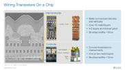
The smallest wires in a chip are the contacts that power the transistor’s gate, source and drain. The contacts connect the transistors to the surrounding interconnect wiring which consists of metal lines and vias that allow power and signals to be routed to transistors and throughout the chip.
To create the wiring, we etch trenches into dielectric material and then deposit the wiring using a metal stack that typically includes a barrier layer that prevents the metal from mixing with the dielectric; a liner layer that promotes adhesion; a seed layer that facilitates metal fill; and a metal like tungsten or cobalt for the transistor contacts and copper for the interconnect wires.
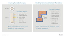
Unfortunately, the barriers and liners don’t scale well, and as we shrink the trench patterns using EUV, the proportion of space consumed by the barriers and liners increases, while the room available for wiring is reduced. And the smaller the wiring, the higher the electrical resistance.
Applied has been developing new technologies that reinvent how chip wiring is engineered and manufactured. At our May 26 Master Class, we will unveil innovations that solve the resistance challenges of EUV scaling.
Improving Logic Scaling with Backside Power Distribution Networks
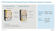
Transistors are powered by a network of wires that transfer voltage from an off-chip regulator through all of the chip’s metal layers and to each logic cell. At each of the chip’s 12 or more metal layers, wiring resistance reduces the supply voltage.
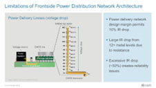
Power delivery networks have a design margin that can tolerate 10-percent voltage drops between the regulator and the transistors. Further scaling the lines and vias with EUV is leading to higher resistance and routing congestion. As a result, we may not be able to scale beyond 3nm using existing power delivery techniques without experiencing voltage drops as high as 50 percent, creating serious transistor reliability issues.
Within each logic cell, the power lines (also called “rails”) need to be a certain size to deliver enough voltage for the transistors to switch. They do not scale as well as other logic cell components such as transistor structures and signal wires. As a result, the power rails are now about three times wider than the other elements, posing a major barrier to logic density scaling.
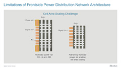
The solution is a simple and elegant idea: since logic wafers are the most valuable real estate on the planet—with a cost now approaching $1 billion per acre—why not move all of the power wiring to the empty real estate on the back side of the wafer, thereby solving both the voltage drop issue and the logic cell scaling dilemma—and dramatically increasing value?
That is exactly what we will do with innovations based on the leadership technologies Applied uses to create wiring on the front side of the wafer. “Backside power delivery networks” will circumvent the chip’s 12 or more wiring levels to reduce the voltage drop by as much as 7X. Removing the power rails from the logic cells can enable logic density to be scaled by up to 30 percent—equivalent to two generations of EUV scaling—at the same lithography pitch.
Based on publicly available information, chipmakers are now evaluating three distinct architectures for backside power delivery, each having design trade-offs. Some approaches will be easier to manufacture, while other, more complex approaches can maximize area scaling. During the Master Class, we will describe these backside power delivery approaches and how Applied’s broad portfolio of materials engineering solutions will help enable the new roadmap.
Heterogeneous Integration Drives PPACt at the Chip and System Level
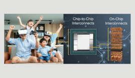
As transistor counts continue to increase exponentially while 2D scaling slows, die sizes are increasing and pushing up against the “reticle limit” which at 858mm2 is the largest mask pattern that can be printed on a wafer. When Moore’s Law was working well, designers could put a large number of high-performance PC and server chips in that space, or a small number of extremely high-performance server chips. Today, designers of server, GPU and even PC chips want more transistors than can be fit inside the reticle field. This forces and accelerates the industry’s transition to heterogeneous design and integration using advanced packaging technologies.

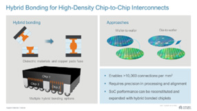
Conceptually, if two chips could be connected using their back-end-of-line interconnect wires, the heterogeneous die could perform as one, overcoming the reticle limit. In fact, this concept exists: it is called hybrid bonding, and it is now emerging on the roadmap of leading chipmakers. A promising example is the ability to bond a large SRAM cache memory chip to a CPU chip to simultaneously overcome the reticle limit, speed development time, increase performance, reduce die sizes, increase yield and reduce cost. The SRAM cache can be built using an older, depreciated manufacturing node to further reduce cost. In addition, using advanced substrates and packaging technologies such as through-silicon vias, designers can bring other technologies that don’t scale well—such as DRAM and flash memory, analog, power and optical chips—closer to the logic and cache memory to improve system design flexibility, cost and time to market, as well as increase system performance, power, size and cost.
To help accelerate the industry’s transition from the System-On-a-Chip era to the System-On-a-Package era, Applied Materials is working on comprehensive solutions for hybrid bonding. During our Master Class, we will detail the hybrid bonding process flow and provide an update on how we are working with our development partners to provide customers with a complete, end-to-end ecosystem of technologies for chip-to-wafer and wafer-to-wafer hybrid bonding.
A related area we will also discuss is the need for larger, semiconductor-grade advanced substrates for heterogeneous integration that allow designers to use substantially larger packages to integrate more chips at a competitive cost.