


Three-dimensional (3D) scanning is a powerful tool that acquires volumetric data leveraged for various metrology, inspection, detection and 3D imaging equipment. Designers frequently opt for structured light systems based on TI DLP technology when they need very fast, high-accuracy scans with millimetre to micron resolution.
The emergence of 3D scanning systems


Simple two-dimensional (2D) inspection systems have been around for many years and generally employ the technique of lighting an object, taking a picture and comparing that image to a known “golden” 2D reference. 3D scanning adds the ability to incorporate volumetric information. Introducing z-dimension data enables measurements of volume, flatness or roughness. The ability to measure these additional geometries—not captured by 2D systems —is critical in industries such as printed circuit board (PCB), solder paste and machined part inspection. It is also used for medical, dental and hearing aid manufacturing.
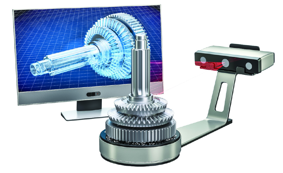
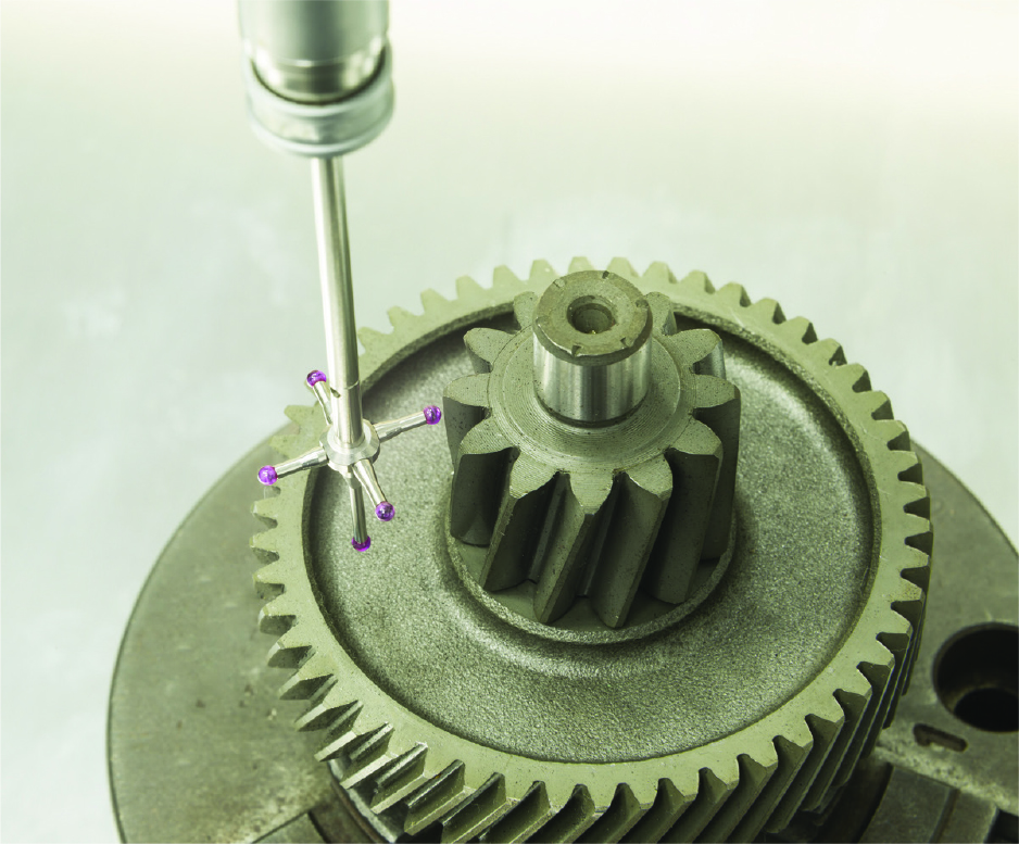
Coordinate measurement machines (CMMs) were one of the first industrial solutions to gather 3D information. A probe physically touches an object’s surface and combines the positional data from each point to create a 3D surface model (Figure 1). Optical methods such as structured light (Figure 2) later emerged for 3D scanning. Structured light is the process of projecting a series of patterns onto an object and capturing the pattern distortion with a camera or sensor. A triangulation algorithm then calculates the data and outputs a 3D point cloud, which becomes the data for various calculations in measurement, inspection, detection, modelling or machine vision systems. Optical 3D scanning is popular because it does not touch the object being measured and can be acquired very quickly, or even in real time.
DLP technology enables fast, smart light pattern generation
For optical 3D scanning equipment, DLP technology is often used in systems as a source for structured light. A DLP chip is an array of highly reflective aluminiummicro mirrors known as a digital micro mirror device (DMD). When combining a DMD with an illumination source and optics, this sophisticated micro-electricalmechanical system (MEMS) can power various projection and spatial light modulation systems.
Designers frequently select DLP technology for structured light applications as the DMD is a flexible, fast, and highly programmable pattern generator. Unlike laser line scanners or diffractive optical elements (DOEs) with a fixed pattern set, it’s possible to program numerous patterns with varying bit depth to a DMD. Structured light solutions using DLP technology are preferable for more detailed measurements that require accuracy in the millimetre or even micron range.
Applications leveraging 3 D scanning systems
3 D AOI
3D automated optical inspection (AOI) is a powerful technique used in manufacturing settings to provide real-time, in-line, decisive measurements relating to part quality. For example, 3D measurements for PCB solder paste inspection (SPI) are highly preferred since they measure the actual volume of solder paste deposited before component placement, helping prevent poor-quality solder joints (Figure 3). PCB manufacturing also leverages 3D AOI in-line after component placement, reflow, final inspection, and rework operations to maximize quality and reliability. As 3D inspection capabilities become more widespread, there are several emerging in-line factory inspection points choosing to take advantage of 3D AOI systems.
Medical
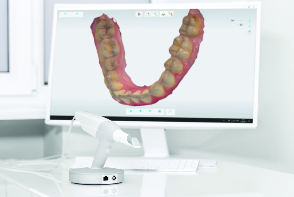
There has been explosive growth using 3D scanning technologies in the medical industry. Intra-oral scanners (IOS), for example capture direct optical impressions in dentistry (Figure 4). Micron-level 3D image accuracy is required to fabricate prosthetic restorations such as inlays, onlays, copings, and crowns. IOSs simplify clinical procedures for dentists, eliminate the need for plaster models and reduce patient discomfort.
Another example of a growth industry is 3D ear scanning. Optical imaging systems capture precise 3D models of ears rather than using silicon ear mold impressions. 3D ear scanning also can enable the future of customization for consumer ear buds, hearing aids, and hearing-protection devices.
Industrial metrology and inspection
There are a multitude of different industrial metrology and inspection systems that have migrated to 3D optical-scanning techniques.
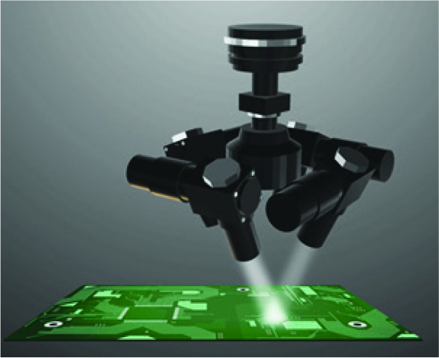
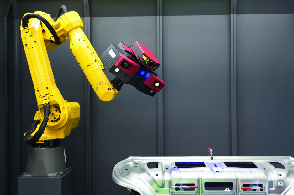
Optical 3D surface inspection microscopes are an example of an alternate option to offline CMM systems. These microscopes can measure more features for height, roughness, and computer-aided design (CAD) data comparison. Factories that build machined, cast, or stamped goods are another area embracing optical inspection. They can more easily and accurately measure x, y, and z dimensions for improvedquality assurance. Inline 3D vision systems combined with robot arms have also emerged in the market (Figure 5). These robotic implementations can greatly increase speed and quality at automotive (Figure 6) and other production-line factories. Adding 3D inspection at specific stages of the assembly and production process can catch quality issues early, thereby reducing waste and rework. 3D scanning systems can even be implemented inside computer numerical controlled (CNC) equipment and 3D printers to enable real-time measurements during the manufacturing process.
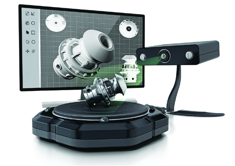
Prosumer 3D scanners
Prosumer 3D scanners are portable tools offering professionals and amateurs the ability to capture complete details of real-world objects in a 3D data format (Figure 7). The data can then be used for product design, part engineering, 3D content creation, or as input to a 3D printer. For example, online retailers can 3D scan their products and present them online in a true, high-quality 3D model instead of 2D pictures. Gamers may 3D scan themselves and create their own avatars in a game.
3 D biometrics identification and authentication
The use of biometric identification and authentication continues to increase. It is often used for securely locking or unlocking devices, security checks, and financial transactions. Using optical 3D scanning technology to capture face, fingerprint or iris biometrics can be a more secure means of identification and makes hacking and other attacks more difficult (Figure 8).

System design benefits when integrating DLP technology
Whether inspecting PCBs for quality or making an accurate dental fitting, 3D scanning equipment using DLP technology for structured light can offer several compelling system benefits. The micro mirrors on a DMD switch very fast—in microseconds—and can enable 8-bit phase shift rates greater than 1,000 patterns per second. This leads to high-speed data capture rates to achieve real-time 3D scans that are very useful for in-line measurements. High-speed DLP chips also offer programming flexibility to dynamically select and reorder patterns on the fly. This helps ensure the optimal pattern is applied to specific object locations or within specific fields of view, which assists in extracting the most accurate 3D information for analysis. Pattern duration and brightness can be controlled, ensuring the optimal amount of light is being reflected from the object and maximizing the dynamic range from the camera.
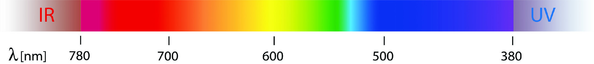
DLP technology can be combined with various light sources and is compatible across ultraviolet (UV), visible and near-infrared (NIR) wavelengths (Figure 9). This offers additional versatility for tailoring 3D scanning systems based on the target object’s reflectivity. The flexibility to combine DLP chips with a broad choice of light sources and diverse camera options makes it possible to easily create one piece of equipment to measure multiple objects. It makes sense that automotive, industrial and medical companies look to DLP chips when designing next-generation 3D scanning equipment.
System integrators are able to innovate with flexible pattern control and new structured light algorithms when designing solutions using DLP technology. They can also optimize optical architectures to match key resolutions and illumination requirements for inspection scans. It is exciting that innovators can take 3D scanning to new levels using advanced programmability to optimize performance in all three of the spectral, spatial and temporal domains.
DLP Products portfolio considerations
TI’s advanced light control portfolio offers DMDs and companion controllers imaging capabilities beyond traditional display. In particular, DMD chips span 363-nm to 2,500-nm wavelength range, have binary pattern rates up to 32 kHz and offer more precise pixel accurate control. Here’s how DLP chipsets with advanced light control can benefit structured light systems.
DMD characteristics
- Resolution:DMD options range from 0.2 to 4.1 megapixels (MP) at the time of this publication. Larger 1, 2, or 4-MP DMDs tend to be used for systems requiring larger scan areas or bright ambient light situations. For instance, automotive 3D inspection requires large scan areas on bright factory floors during assembly and alignment process steps. DMDs less than 1-MP tend to be placed in compact handheld or tabletop equipment that requires portability or low power consumption.
- Power:The smallest chipsets use less than 200-mW of power consumption, making them a good fit for portable or battery-operated systems. Intra-oral scanning, for example, takes advantage of small DMD form factors with low power consumption for battery-powered implementations.
- Wavelength:Users have the ability to adjust colour and illumination intensity in a DLP technology-based system based on an object’s reflective properties. This is made possible since a DMD can be combined with various light sources, including lamps, light-emitting diodes (LEDs) and lasers. There are DMDs optimized for UV (363–420-nm), visible (400–700-nm), and NIR (700–2,500-nm) use. For biometric 3D scanning solutions, near-infrared wavelengths are popular because the scans are not invasive. UV light is sometimes best for optimizing metals’ reflective properties. For white light patterns, white LED optical engines are a desired power-efficient monochrome solution.
Controller characteristics
Pre-stored patterns:DLP controllers provide convenient interfaces for reliable, high-speed DMD control. They support pre-stored structured light patterns without the need for an external video processor to stream patterns. Some DLP controllers can pre-store more than 1,000 structured light row or column patterns using one-dimensional (1D) encoding (see Figure 10 for example). 1D patterns take advantage of using a single row or column and repeating that row or column across the entire array. Prosumer 3D scanner products often use 1D patterns to help reduce cost and increase scanning speed. More advanced controllers support up to 400 pre-stored 2D full-frame patterns (see Figure 11 for example), which can be more tailored in x and y depending on the application needs or objects being scanned.
Pattern accuracy and speed: DLP controllers are designed to display patterns suitable for machine vision or digital exposure and support variable high-speed pattern display rates up to 32,000 patterns per second with camera synchronization. These pattern rates are critical for highly accurate and high-speed 3D scanning systems.
From simple to complex systems, DLP technology offers customers incredible pattern flexibility when they design their custom structured light system hardware and algorithms.
Summary
3D scanning using structured light is a desirable technique for the expanding markets and use cases requiring 3D optical measurement. Texas Instruments offers a diverse portfolio of DLP chips that can enable small, integrated scanning engines in personal electronics up to large, high-resolution pattern generators used in industrial inspection systems. DLP technology is a predominant technology choice for 3D scanning and machine vision solutions due to its tremendous versatility to customize patterns at very high speeds and its ability to pair with multiple light sources and wavelengths. This versatility also drives customer innovation and can push 3D scanning system capabilities to new limits.