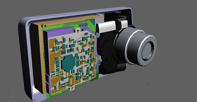
The focus of CR-8000 2018, according to the Zuken, is on enabling efficient front-loading of design constraints and specifications to the design creation process, coupled with sophisticated placement and routing capabilities for physical layout.
“With smart applications adding complexity to the product design process, controlling adherence of PCB designs to engineering and manufacturing specifications is a critical activity in advanced PCB design,” said Zuken chief strategy officer Humair Mandavia. “By providing more intelligent and automated features necessary to drive specification and communication of constraints and guidelines, Zuken wins back valuable time in the PCB design chain”, he added.
Front-loading of design intent from Design Gateway to Design Force has been achieved by adding a unified constraint browser for both applications, enabling hardware engineers to assign topology templates, modify differential signals and assign clearance classes to individual signals.
Using a rule stack editor during the circuit design phase, hardware engineers can now load design rules that include differential pair routing and routing width stacks directly from the design rule library into their schematic. Here they can modify and assign selected rules for cross talk and differential pair control.
An enhanced component browser enables component variants to be managed in the schematic, and assigned in a user-friendly table.
Manual routing is supported by an ‘auto complete and route’ function, and designers also have the option to look for paths on different layers while automatically inserting vias.
A new bus routing function allows paths to be sketched for multiple nets to be routed over dense areas. “An added benefit is the routing of individual signals to the correct signal length as per the hardware engineer’s front loaded constraints, to meet timing skew and budgets,” said the firm. If modifications to fully placed and routed boards are required, an automatic re-route function allows connected component pins to remain connected with a re-route operation during the move process.
Automatic stitching of vias in poured conductive areas can be specified by inside area on-line, perimeter outline or both inside and perimeter.
Design-for-manufacturing (DFM) has been enhanced to include checks for non-conductor items, such as silkscreen and assembly drawing placed reference designators. A design rule check will make sure component reference designators are listed in the same order as the parts for visual inspection accuracy.


