


Historically, there have been preferred methods of power conversion from AC to DC and DC to DC. These have been set by a variety of constraints that have evolved over time. There was a day, for example, when ‘power factor correction was only implemented in AC distribution and an AC/DC power supply could happily have a PF of 0.6 or even lower. Statutory limits came in around 1982 in Europe. As a result, ‘mains harmonic suppression,’ as it’s more accurately called, is required for some equipment, such as power supplies with a rated power of over 75W but is lower in some applications such as lighting. This practically involved adding another ‘boost’ power conversion stage to every AC/DC, to the chagrin of manufacturers, although it did enable other features such as universal input and long-ride-through times. The first circuits involved an input inductor, switch, and rectifier diode and were not very efficient. Similarly, DC/DC conversion stages within an AC/DC over 100W or so started as simple forward converters in the form of half- or full-bridges—relatively easy to understand and implement but with limited efficiency due to the semiconductor technology available and the ‘hard-switching’ nature of the topologies.
Performance specifications, such as the 80 PLUS certification program from around 2004, have made these basic PFC and DC/DC conversion topologies non-viable for the efficiency levels demanded: For example, the highest ‘Titanium’ level requires 96 percent efficiency at 50 percent load for 230VAC equipment. New techniques have therefore evolved, and today, a popular combination, viable up to several kW, for high power density and efficiency is a ‘Totem pole PFC’ (TPPFC) stage followed by a resonant ‘CLLC’ converter.


The Totem Pole PFC Stage
The TPPFC effectively eliminates the input bridge rectifier in an AC/DC front end by using semiconductor switches as synchronous rectifiers (Figure 1). At medium to high powers, the circuit is operated in ‘Continuous Conduction Mode’ to keep peak current manageable, which results in ‘hard switching’.
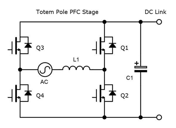
On one mains polarity, Q1 acts as a diode and Q2 as a high-frequency boost switch, and on the other polarity, the functions swap. Q3 and Q4 act as synchronous diodes providing a path for AC line current to return to the supply and could be discrete diodes for a lower cost. It’s clear that there are only switches in the power path, here shown as SiC FETs, so conduction losses are set only by device on-resistances. If Si-MOSFETs were used for Q1 and Q2, the reverse recovery of their body diodes, which conduct during dead time, would limit the efficiency achievable. However, with SiC FETs in these positions, such as the latest 750V Gen 4 18mΩ parts from UnitedSiC (now Qorvo), a 99.3 percent semiconductor efficiency can be achieved at 6.6kW output, switched at 75kHz, and just 8.3W lost in each of Q1 and Q2. This is due to their market-leading on-resistance and extremely low recovery losses.
The CLLC DC/DC Converter
With a target of 96 percent overall efficiency, the TPPFC stage is a great start. For the main DC/DC isolation stage, the benefits of a resonant converter can be leveraged with the popular ‘CLLC’ type (Figure 2).
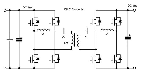
The CLLC is a variable frequency converter with a 50 percent duty cycle drive to each switch and is symmetrical, so that it can be used for bi-directional conversion. The topology is resonant, so it can achieve zero-voltage switching on the primary and zero current and zero-voltage switching on the secondary. In a resonant converter, switching losses are very low and body diode recovery is not an issue, so frequency can be pushed up to minimize magnetics size. Nevertheless, there is a limit to this influenced by the output capacitance of the device, which dictates the minimum ‘dead’ time and operating range. Again, SiC FETs are an ideal choice, with the best figure of merit for specific output capacitance and on-resistance on the market at high and low temperatures, as well as a very low body diode forward voltage drop, resulting in excellent efficiency. For example, at 300kHz, 6.6kW, the same UnitedSiC Gen 4 parts as used in the example PFC stage yield 99.8 percent semiconductor efficiency. An additional benefit of SiC FETs is their easy 0-12V gate drive.
UnitedSiC has developed a range of 750V Gen 4 SiC FET parts with optional packages and on-resistances so that designers have a wide choice to suit their performance targets and budgets. All the options can be explored with the company’s online FET-Jet Calculator, which gives instantaneous performance results for SiC FETs in a wide range of selectable topologies, including the TPPFC and CLLC. The power dissipated, the temperature rises, and component stress levels are indicated, with the user able to specify electrical and thermal operating conditions along with the effect of paralleling multiple parts.
Do we have the ultimate topologies and switches now? With stage efficiencies now only a small fraction of a percent away from 100%, we are pretty close.
Courtesy: Mouser