


Introduction
This one started last year with me just messing around on a windy, rain-swept day, seeing if I could do something simple with a JFET. It’s taken quite a while to make it to the blog: I dropped it, started it again, stalled, and have now, eventually, finished it. [It was also leap-frogged by the regulator-as-an-oscillator one, which you’ll notice had quite a lot in common with this one.]


What I was trying for was an oscillator that had an output frequency of several hundred kilohertz and where the frequency could be varied by perhaps 10kHz or so by adding a modest amount of capacitance, say up to about 50pF max. Take note that I don’t really know what I’m doing with all this analog stuff, so don’t read it as a tutorial because, whatever it is, it’s certainly not that. Comments are welcome, particularly if you can tell me how I should be doing this.
For the gain element, I’m going to use a JFET. That’s because this is a follow-on from some of the JFET blogs I did a little while back and I’m currently interested in how they work. I’ve used a BF256B n-channel part simply because I have some. According to the datasheet, that part was originally ‘designed for VHF/UHF amplifiers’ so it shouldn’t have any problem at all oscillating at 200kHz.
I’ve chosen a Colpitts type circuit for the frequency-selective network. This incorporates an LC tuned circuit with the capacitor split to provide a tap for the feedback. Whether that’s a good choice, I don’t know. An alternative arrangement would be to split the inductor (that one’s called a Hartley oscillator), but the Colpitts seemed simpler. There’s also a further variation on the Colpitts called a Clapp oscillator; I might take a look at that one in a subsequent blog.
The Circuit
I haven’t designed this from scratch myself, instead I based it on a circuit that I had previously spotted somewhere. I could remember the circuit shape but not any of the component values. My choices might not be very good ones.
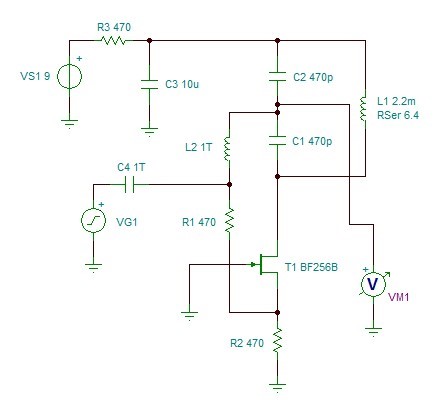
Here is the general form of it
The JFET in that circuit is set up as a common-gate amplifier. That means that the gate terminal is common to both the input and the output signals (one of the terminals has to be common to both input and output because the device only has three terminals). The input is applied to the source terminal and the output is taken from the drain terminal. If you’re only used to the common-source [or common-emitter for a BJT] configuration it will look a bit odd, but it’s a perfectly valid way to use the device. When we talk about configurations like this (common-source, common-gate, or source-follower), we’re talking about circuit configurations and, more specifically, how ac signals
see the circuit. The active device itself just works the way it always works, it doesn’t work in a different way for each configuration, and we need to make sure that the dc biasing, necessary for it to operate at all, functions properly, irrespective of how the ac signals view matters.
In this circuit, the LC circuit forms the output load at the drain. Because current needs to run down through the JFET to bias it correctly, the load goes up to the rail rather than down to ground. To an ac signal, the rail can be considered as more or less the same thing as ground: at higher frequencies, the decoupling capacitors should look much like a short circuit between the two. It also satisfies the dc conditions because, at start-up, even before the oscillation gets going, drain current has a path through the coil.
The resistor from the source to ground sets the bias point of the device. Arranged like this, the JFET self-biases. It looks a bit odd on a circuit, but once you understand it it’s quite straightforward.
Here it is in the simulator
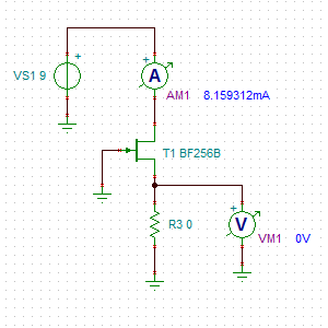
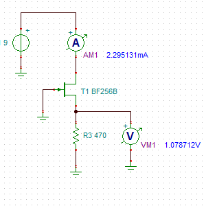
With zero ohms, the current is the Idss value. The simulator thinks that it is about 8mA. That’s reasonably close to the values I get with my bag of JFETs which are something like 9mA. With 470R, it’s just over 2mA, giving a voltage at the source of around 1V. I decided to go with that for the circuit. I can live with 1V at the source and 2mA is a reasonable figure for the standing current. It might not be obvious, but the JFET regulates that current, and hence the voltage at the source. If it increases, the voltage between source and ground increases and then the gate going more negative (relative to the source) has the effect of reducing the current. If it decreases, the voltage between source and ground declines, the gate is relatively less negative, and the current will increase.
A consequence of using the common-gate configuration and having that resistor there at the input is that it becomes the input resistance and, since it will only be a few hundred ohms, that makes it a fairly low input resistance for an amplifier.
When choosing the L and the C, I have a choice as to the values. As I want to be able to change the frequency quite significantly, maybe by about 5% from the nominal frequency with just a comparatively small amount of additional capacitance, I need to keep the capacitance fairly low and go for a higher value coil to get the frequency I want. I’ve got some 470pF capacitors, so I can have two in series for the capacitor side, giving a capacitance of 235pF. If I put those together with a 2.2mH inductor, the resonant frequency is going to be 221kHz, which is about where I want it. That frequency won’t be the exact frequency of oscillation for a couple of reasons. One is additional circuit parasitic capacitances and inductances that I’m not taking into account. Another is that the oscillation won’t take place at exactly the point where the tuned circuit looks real, and introduces no phase shift, because the criteria is for the full loop and not simply the tuned circuit.
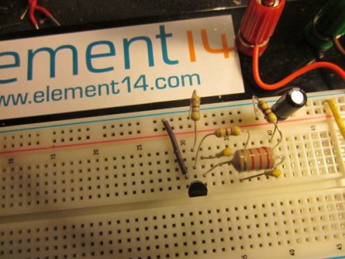
The Breadboard
Here it is, thrown together quickly on a breadboard:
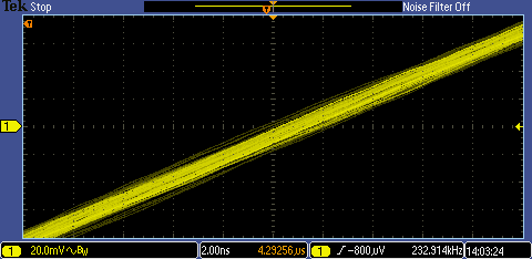
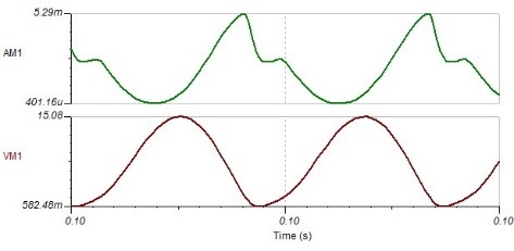
Fortunately, it does actually oscillate. The yellow trace is the signal at the drain of the JFET. The blue trace is the signal at the source.
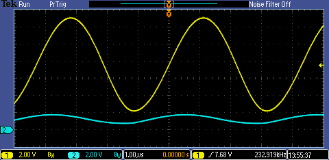
But it’s noticeable, even just looking at the trace, that the output isn’t a very good sinewave [look at the bottom of the yellow trace, where it starts to come back up again, and you can see how it is misshapen]. If I look at it as an FFT on the oscilloscope I can get an idea of the extent of the distortion:
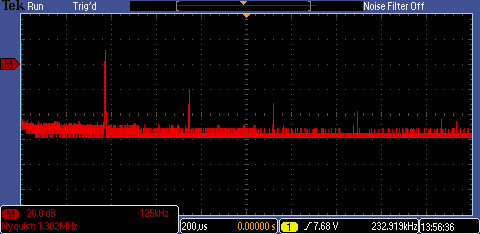
As well as the fundamental, we also have ALL the harmonics in declining proportion. As a THD [Total Harmonic Distortion] figure, that would easily be several percent. I can see two reasons for that. One is that we’re operating the JFET with a large signal and suffering from the non-linearity that comes from the gm [forward transconductance] varying as the bias point of the transistor moves around. The other is down to the crude way the waveform limits.
Time-wise, it’s moderately stable – better than I would have expected for something so simple. If I trigger on it and then look at the next point where it has the same amplitude as the trigger point, one cycle on from the trigger, I see a variation of about plus or minus 1ns.
Here’s how it behaves at start-up:
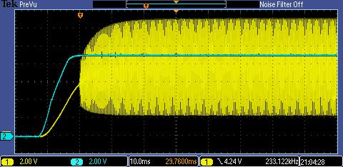
the yellow trace is the signal at the drain, the blue trace is the voltage from the bench power supply as it comes up. It always seems to start reliably; I haven’t had it fail yet. (Don’t worry that the yellow trace looks a bit of a mess in the picture: that’s simply aliasing in the way that the ‘scope presents the display. The overall envelope that the trace shows will be fairly accurate.) Incidentally, that trace emphasises how, because of the tuned, resonant circuit, the drain waveform climbs above the power rail.
Looking at the Circuit in the Simulator
Here I’m simulating the circuit in TI-TINA. These are the equivalent waveforms to the oscilloscope ones above.
the shapes are similar, but there is some difference. I would imagine that’s mostly the difference between the JFET model and the real device.
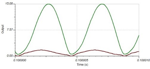
If I put an ammeter in series with the drain on the simulation, we can immediately see how the distortion arises
This is a somewhat non-linear circuit, with the JFET sending pulses of current to the tuned circuit. Potentially, that could be a good thing. Apparently, for good waveform shape and low phase noise, a good approach is to let the tuned circuit do all the work and just give it a short nudge, once a cycle, away from the important timing points, a bit like gently pushing a child’s swing at the top of the arc. In this case, though, it’s more like intercepting the swing before it reaches the top and forcefully sending it back.
Opening the Loop
To understand better how the circuit behaves (in a simulator, so only as good as the models involved), one approach I have is to open the loop. This won’t be simulating the breadboard circuit at all accurately because the physical circuit is working with very large signals whereas the simulation will be working small-signal and won’t be seeing the large-signal distortion, but for all that it might show some useful things to us.
Here’s the circuit. You can see I’ve added two additional components, a capacitor and an inductor, and two test items, a voltage generator to provide a swept input and a voltmeter to record the output.
The two added components don’t affect the way the circuit operates, instead they allow us to trick the simulator. For DC, the simulator will calculate the operating points as though the loop were closed, for AC, the simulator will then give the response as though the loop were open.
Here is the Bode plot I get:
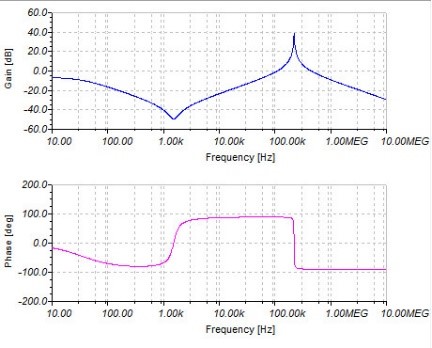
That shows us a nice sharp resonance at a couple of hundred kilohertz and a softer antiresonance at a much lower frequency that isn’t of much consequence because there’s no loop gain there. The LC circuit is responsible for the resonance peak at just over 200kHz. At that point the phase abruptly changes, passing through zero as the LC circuit changes from looking inductive to capacitive. That gives us our two criteria for oscillation, a frequency where the phase shift can settle to zero and where there is also gain of more than one so that the oscillation is sustained (ie at or above 0dB on the gain graph). The rapid way the phase changes shows why an LC tuned circuit like this is good at determining an oscillator frequency.
Here is a more detailed view
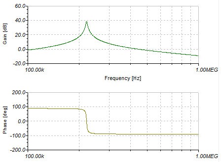
That’s reasonably close to where the oscillation frequency actually was. It’s also useful because it appears to show that there isn’t too much likelihood of the circuit oscillating at the wrong frequency because of the way the gain falls off away from the resonance point. [I have to be careful here because, as I said, I’m not simulating the large-signal oscillation of the actual circuit. Also, JFET parameters vary widely between different batches of the parts, so the typical figures in the simulator’s model might not be very close to the actual devices I’ve got.]
Conclusions
I ended up with something that oscillates, it starts reasonably well, and it seems fairly stable. The waveform isn’t anything to write home about – quite a poor sinewave – but, given the very small number of components, I don’t suppose I should complain too much about that.