Accurate digital temperature measurements are important in a range of applications including wearables, medical monitoring devices, health and fitness trackers, cold chain and environmental monitoring, and industrial computing systems. While widely applied, the implementation of highly accurate digital temperature measurements frequently involves temperature sensor calibration or linearization, as well as higher power consumption which can be an issue for compact, ultra-low power applications with multiple acquisition modes. The design challenges can quickly mount, causing cost overruns and delayed schedules.
Complicating the matter, some applications involve multiple temperature sensors sharing a single communication bus. In addition, some production test setups need to be calibrated according to the U.S. National Institute of Standards and Technology (NIST), while verification equipment needs to be calibrated by an ISO/IEC-17025 accredited laboratory. Suddenly, what seemed a straightforward function becomes both intimidating and costly.


This article briefly describes the requirements for high-accuracy temperature measurements in mobile and battery-powered health monitoring applications. It then introduces a low-power, high-accuracy digital temperature sensor IC from ams OSRAM that doesn’t require calibration or linearization. It finishes with integration recommendations, an evaluation board, and a Bluetooth-enabled demo kit with a companion app that makes it possible to modify sensor settings and observe the impact on power consumption.
Requirements for high-accuracy temperature monitoring
Accuracy is mandatory in health monitoring applications. As manufactured, digital temperature sensors exhibit part-to-part variations in performance that need to be addressed. As in-house calibration is expensive and using uncalibrated sensors increases the cost of achieving the desired accuracy, designers should consider sensors that are fully calibrated and linearized. It is, however, important to ensure that the sensor maker uses calibration instruments traceable to NIST standards. Using instruments with traceable calibration ensures an unbroken chain back to the basic NIST standards, with the uncertainties at each link in the chain identified and documented so they can be addressed in the device maker’s quality assurance system.
The primary standard for testing and calibration laboratories is ISO/IEC 17025 “General requirements for the competence of testing and calibration laboratories.” ISO/IEC 17025 is based on technical principles focused specifically on calibration and testing laboratories, is used for their accreditation, and provides the basis for developing continuous improvement plans.
Digital temperature sensor with NIST-traceable production testing
To meet the many design and certification requirements, designers can turn to the AS6211 digital temperature sensor from ams OSRAM that provides accuracy up to ±0.09°C and requires no calibration or linearization. Designed for use in healthcare devices, wearables and other applications that require high-performance thermal information, the AS6211’s production testing is calibrated by an ISO/IEC-17025 accredited laboratory according to NIST standards. The calibrated production testing speeds the process of gaining certification to EN 12470-3, which is required for medical thermometers in the European Union.
The AS6211 is a complete digital temperature sensor in a six-pin, 1.5 x 1.0-millimeter (mm) wafer level chip scale package (WLCSP), ready for system integration. An orderable part number example, the AS6221-AWLT-S, is delivered in lots of 500 pieces on tape & reel. The AS6211’s measurements are delivered through a standard I²C interface, and it supports eight I²C addresses, thereby eliminating concerns about bus conflicts in multi-sensor designs.
High accuracy plus low power
The AS6221 delivers high accuracy with low power consumption over its full supply range from 1.71 to 3.6 volts DC, which is especially important in applications powered by a single battery cell. It includes a sensitive and accurate silicon (Si) bandgap temperature sensor, an analog-to-digital converter, and a digital signal processor with associated registers and control logic. The integrated alert function can trigger an interrupt at a specific temperature threshold, which is programmed by setting a register value.
The AS6221 consumes 6 microamperes (µA) when making four measurements per second, and in standby mode, power consumption is only 0.1 µA. The use of the integrated alarm function to wake up the application processor only when a temperature threshold has been reached can reduce system power consumption even more.
Wearables integration options
In wearable applications, the better the thermal connection between the sensor and the skin, the more accurate the temperature measurement. Designers have several options for optimizing the thermal connection. One way is to put a thermally conductive pin between the skin and the sensor (Figure 1). To achieve reliable results, the pin needs to be isolated from any external sources of thermal energy, such as the device case, and a thermal paste or adhesive should be used between the pin and the AS6211. This approach benefits from using a flexible (flex) printed circuit board (PCB) to carry the AS6221, enabling more freedom in locating the sensor.
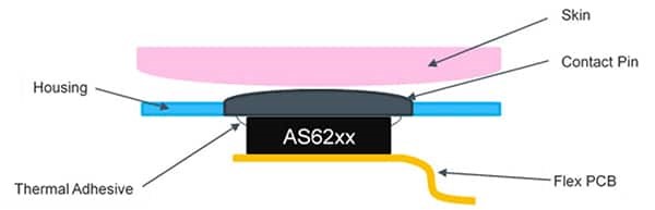
Figure 1: A flex PCB and thermal adhesive can be used to provide a low thermal impedance path between the skin and the sensor.
In designs that benefit from having the sensor on the main PCB, the thermal connection can be made using a contact spring or a thermal pad. If the sensor is mounted on the bottom of the PCB, a contact spring can be used to make a thermal connection between the contact pin and thermal vias on the PCB that are connected to the sensor (Figure 2). This approach can result in a cost-effective device that supports longer distances between the sensor and the skin, but it requires careful consideration of the several thermal interfaces to achieve high levels of sensitivity.
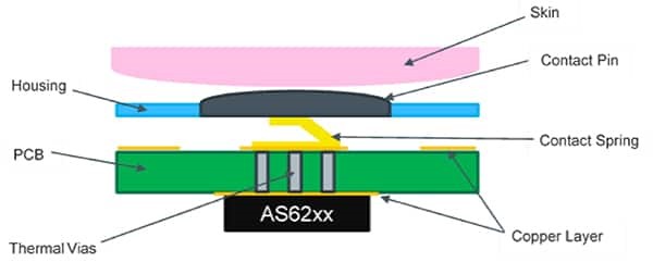
Figure 2: When the sensor is mounted on the bottom of a PCB, thermal vias and a contact spring can be used to connect to the contact pin.
A third option is to use a thermal pad to connect the pin to a sensor mounted on the top of the PCB (Figure 3). Compared with using a spring contact or flex PCB, this approach requires a pad with high thermal conductivity and careful mechanical design to ensure minimum thermal impedance between the contact pin and the sensor. This can result in a simpler assembly while still delivering high levels of performance.
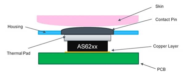
Figure 3: A thermal pad can connect a top-mounted sensor to the contact pin. This provides simpler assembly, while still delivering high performance.
Improving thermal response time
In order to obtain fast thermal response times, it’s important to minimize the external influences on the measurement, especially by the portion of PCB directly adjacent to the sensor. Two viable design suggestions are to use cutouts to minimize any copper planes in the vicinity of the sensor on the top of the PCB (Figure 4, top), and to reduce thermal loading from the bottom of the PCB by using a cutout area below the sensor to reduce overall PCB mass (Figure 4, bottom).
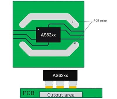
Figure 4: Cutouts on the top and bottom of the PCB can minimize the PCB mass around the sensor and improve its response time.
In addition to minimizing PCB effects, other techniques that can help improve measurement speed and performance include:
- Maximizing the contact area with the skin to increase the heat available to the sensor.
- Using thin copper traces and minimizing the size of power and ground planes.
- Using batteries and other components such as displays that are as small as possible to achieve the device performance requirements.
- Designing the package to thermally isolate the sensor on the PCB from the surrounding components and the outside environment.
Sensing environmental temperature
Additional considerations apply when using multiple temperature sensors, such as in designs that use both skin temperature and the temperature of the surrounding environment. A separate sensor should be used for each measurement. The thermal design of the device should maximize the thermal impedance between the two sensors (Figure 5). A higher intervening thermal impedance provides better isolation between the sensors and ensures that the measurements will not interfere with one another. The device package should be fabricated with materials that have low thermal conductivities, and a thermal isolation barrier should be inserted between the two sensor sections.
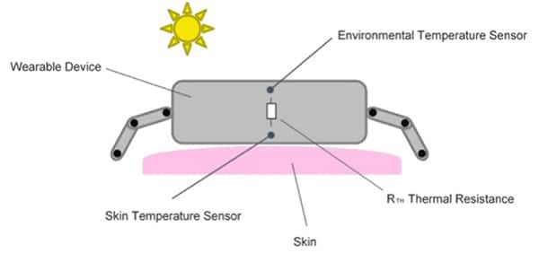
Figure 5: For accurate environmental temperature sensing, there should be a high thermal resistance between the skin and environmental temperature sensors.
Eval kit kickstarts AS6221 development
To speed application development and time to market, ams OSRAM offers designers both an eval kit and a demo kit. The AS62xx Eval Kit can be used to quickly set up the AS6221 digital temperature sensor, enabling a quick evaluation of its capabilities. This eval kit connects directly to an external microcontroller (MCU) that can be used to access temperature measurements.

Figure 6: The AS62xx eval kit can be used to set up and evaluate the AS6221
Demo kit for the AS6221
Once the basic evaluation is completed, designers can turn to the AS6221 demo kit as an application development platform. The demo kit includes an AS6221 temperature button and a CR2023 coin cell battery. Downloading the companion app from the App Store or Google Play Store supports connection to up to three sensor buttons at one time (Figure 7). The app communicates with the sensor buttons over Bluetooth, making it possible to modify all of the sensor settings, including the measurement frequency, and observe the impact on power consumption. The app can record measurement sequences, thereby enabling comparisons of the performance of various temperature sensor settings. Designers can also use the demo kit to experiment with the alert mode and learn how it can be used to improve solution performance.
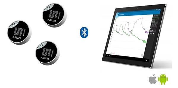
Figure 7: The AS6221 demo kit serves as a temperature sensor application development platform for the AS6221.
Conclusion
Designing high-accuracy digital temperature sensing systems for healthcare, fitness, and other wearables is a complex process with respect to design, test, and certification. To simplify the process, lower cost, and get to market more quickly, designers can use highly integrated, low-power, high-accuracy sensors.