


Automotive, General, Power by onsemi
(Source: onsemi)


High-side SmartFETs have grown in popularity due to their ease of use and the high level of protection. Like standard MOSFETs, SmartFETs are ideal for various automotive applications. What separates them is the control circuitry built into a high-side SmartFET device. The control circuitry constantly monitors output current and device temperature while offering passive protection against voltage transients and other unexpected application conditions. This combination of active and passive protection features ensures a robust application solution, extending the lifetime of both the device itself and the application load it is protecting.
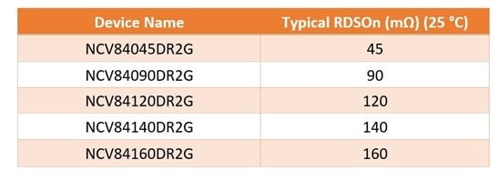
Onsemi now offers a family of high-side SmartFETs ranging from 45mΩ up to 160mΩ. The devices are protected, single-channel high-side drivers that can switch various loads, such as bulbs, solenoids, and other actuators. As shown in Table 1, the device name indicates the typical RDSOn of the SmartFET at 25°C. The complete family of products is listed below:
Table 1: The Complete Family of onsemi High-Side SmartFETs
onsemi’s family of devices is housed in an SO8 package, providing a small footprint while delivering high power. A family pinout for the 45mΩ to 140mΩ devices provides convenience to the designer, allowing one pinout for various application load uses. Simply switch out one device for another depending on the level of current required for a given application. The devices drive 12V automotive grounded loads and provide protection and diagnostic capabilities. The family of devices incorporates advanced protection features such as active inrush current management, over-temperature shutdown with automatic restart, and an active overvoltage clamp. A dedicated Current Sense pin provides precision analog current monitoring of the output and fault indication of short to battery, short circuit to ground, and ON and OFF state open load detection. All diagnostic and current sense features can be disabled or enabled by an active-high Current Sense Disable pin (NCV84160 only), or an active-high Current Sense Enable pin (all other parts in the family).
The “end requirement” from a high-side SmartFET is to switch loads, and there are different alternatives available in the market towards that end. Relays, for instance, have been used for a long time in the industry to switch various automotive loads, especially those requiring high current activation. With a continual reduction in the weight and size of automotive components and assemblies, there has been a transition from relays to semiconductor switches that take up less area and offer improved noise immunity and lower electromagnetic interference than relays.
High-side SmartFETs have become the dominant SmartFET configuration in the automotive market, replacing the generally simpler low-side SmartFET. Figure 1 shows an example of a high-side versus low-side SmartFET configuration. While a high-side SmartFET’s load always connects to the ground with a switched connection to the supply, a low-side SmartFET’S load always connects to the power supply with a switched connection to GND. The SmartFET is typically housed inside a control unit or ECU. The load line is the cable length that connects the load to the pin connector on the ECU. Depending on the load type and its location in the vehicle, this load line could belong, thereby increasing the likelihood of a short to chassis ground which could be a severely stressful condition for the load in a low-side SmartFET configuration. This makes the high-side SmartFET the preferred choice for load switching.
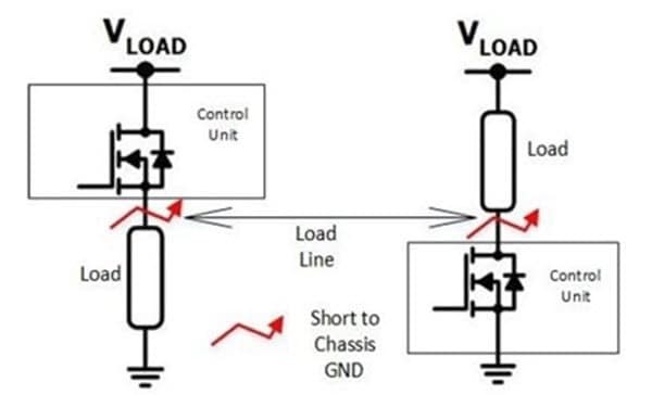
Figure 1: High-Side Versus Low-side Switch in an Application (Source: onsemi)
Figure 2 below shows the top-level block diagram and pin configuration of the NCV84xxx high-side SmartFET family from onsemi. Notice that the high-side SmartFET is, in fact, an NMOS FET, with a Regulated Charge Pump pulling the gate voltage up high enough to drive the load.
The Input (IN) pin is a logic level pin that turns the control logic/charge pump on and off to operate the FET. The Current Sense Enable (CS_EN) pin enables and disables the Current Sense feature. The Current Sense (CS) pin allows proportional load current sensing to be fed back to the microcontroller for real-time feedback. This pin is multiplexed; it reports analog fault events, which are easily distinguishable from normal operation, giving the user the capability of sensing the output current or a fault condition in real-time. The voltage (VD) pin connects directly to the battery or power supply, and the OUT pin connects to the load. Finally, the ground (GND) pin is simply the device GND.
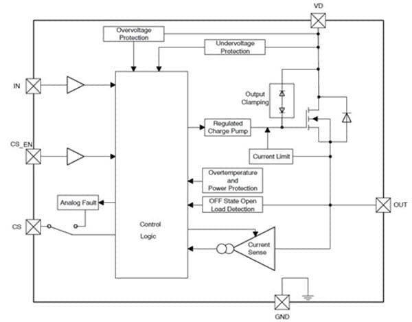
Figure 2: Block Diagram and Pin Configuration of NCV84xxx (Source: onsemi)
The NCV84xxx SmartFET family of devices offers the following protection features:
- Over Voltage Protectionprotects the entire device clamping VD-GND for voltages > 41V.
- Undervoltage protection,in case of a low battery voltage, turns the device off and waits until the battery voltage has risen high enough to operate the Regulated Charge Pump to run the FET properly.
- Current Limit (see Figure 3below) limits the current in case of a short-circuit or in-rush event to prevent damage. The current will stay limited until the internal die temperature of the device exceeds the overtemperature point and will turn itself off for protection until it has cooled down enough. This feature is excellent for driving bulb loads that require a high initial inrush current, and it also limits the amount of stress on the die from high power and temperature swings.
- Overtemperature and Power Protection with Auto-Restartprotect the device from overheating due to high power dissipation and excessive ambient temperature rise. If overtemperature protection is activated, the device will shut itself off until it cools enough and auto-retry, assuming the input is “high.”
- OFF-State Open Load Detection alerts the microcontroller that the connection to the load has been lost in the Off-State before turning the input “high.”
- Output Clamping for Inductive Load Switching during an inductive discharge event, the output clamp will safely turn the FET on to handle the inductive discharge current.
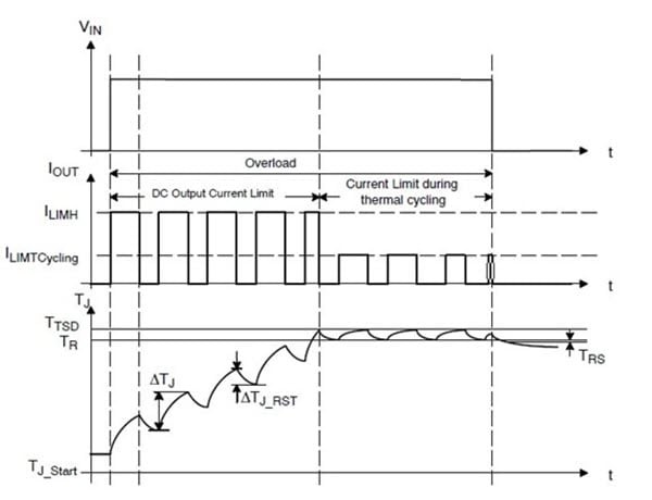
Figure 3: How TJ Progresses During Short to GND/Overload (Source: onsemi)
For in-depth information on how the high-side SmartFETs operate, including protection functions, current sensing, etc., please refer to onsemi’s application note—High-Side SmartFET with Analog Current Sense Application Note.
Source: https://www.mouser.in/blog/highside-smartfet-drivers-automotive-load-applications
Additional Resources:
- High-Side SmartFET Demonstration Console Demo video
- NCV84045 Product Page
- NCV84090 Product Page
- NCV84120 Product Page
- NCV84140 Product Page
- NCV84160 Product Page
The High-Side SmartFET Drivers for Automotive Load Applications blog was first published on onsemi.com and was reposted here with permission.