


The fully differential amplifier (FDA) has emerged as a very popular last-stage interface to differential-input analog-to-digital converters (ADCs) spanning the range from 24-bit delta-sigma, 18- to 20-bit successive approximation register (SAR), through to 14- to 16-bit pipeline designs.
An accurate output-noise calculation enables designers to compare alternate FDA designs. Combining the differential spot noise at the output pins of the FDA with any passive filtering to the ADC allows you to make an accurate signal-to-noise ratio (SNR) calculation up to the ADC. And by combining the FDA-plus-filter SNR and ADC SNR, you can accurately predict the expected SNR degradation over ADC-only data sheet specifications.


This article will step through the calculations of FDA output spot noise, including 1/f effects showing interstage passive filtering and their effect on band-limiting the integrated noise, and show example designs using calculated, measured and simulated results.
Developing an accurate differential-output spot-noise expression for any FDA design
While many resources describe the output-noise calculation for an FDA [1], [2], [3], a refresher showing the importance of resistor-noise terms and how to include 1/f effects will give you a solid foundation for comparing different solutions. FDAs can take either a single-ended or differential source to differential outputs centered on the required output common-mode voltage for the analog-to-digital converter (ADC) being driven. In this article, the single to differential case will be the focus. Differential input designs are a subset of single-ended input designs for noise-analysis purposes.
Every designer needs to eventually select resistor values where making the following assumptions will lead to good solutions:
- The feedback resistors are equal and set in a range suitable to the FDA you’re considering.
- The total DC and AC source impedance looking back from the FDA summing junctions are matched as well as possible. The two impedance dividers from the output pins to the input summing junctions on each side of the FDA need to match in order to avoid residual “signal-related” output common-mode signals arising from mismatched dividers. Ideally, the output average (or common-mode) level is a fixed DC level set by the Vocm control input signal.
Getting to the lowest total output noise will often suggest the lowest resistor values possible. In FDAs, getting to the lowest noise starts by reducing the feedback resistor target and then scaling the input resistors for the target gain. Just scaling the feedback Rs down will eventually result in loading and excess power-dissipation concerns, while scaling them up will eventually result in phase-margin loss due to the interaction with the FDA input capacitance [1, section 8.2]. For voltage-feedback-type FDAs, the typical approach is to target R values that yield similar or slightly lower output-noise power contributions compared to the output noise produced by the FDA’s intrinsic differential-input voltage-noise specification.
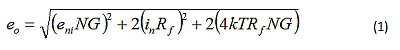
Figure 1 shows the fundamental analysis circuit [1, section 8.3] for an FDA output-noise calculation using equal Rf and Rg assumptions. Equation 1 results from the simplification of the exact expressions (with imbalanced feedback ratios) to equal βs [3].
My recommendations include:
- Reducing the circuit to its simplest form, collapsing all input side networks into a single equivalent resistance.
- Not considering feedback capacitors at this point – they are often added to band-limit the signal path and will also impact the frequency response for the different FDA output-noise terms. To compare different FDA solutions, leave these out for now.
- Assuming that the input current noise and all resistor noise terms are uncorrelated.
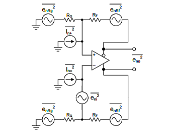
Figure 1 shows the noise terms as powers, but the analysis starts by getting each voltage- or current-noise terms’ gain to output. The output-referred noise terms are combined as a root sum of squares (RSS) of their independent noise-power contributions. Table 1 summarizes the gains for each term.
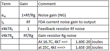
Similar to basic operational amplifier output-noise calculations [4], each term is provided a gain to the output in order to develop a differential voltage-noise term. Each of those terms are squared to combine noise as powers, and taking the square root of the sum of powers gets you back to the differential-output spot-noise voltage. For an FDA, the current-noise and resistor-noise terms on each side will create a 2x factor on the noise powers, as shown in Equation 1.
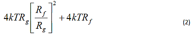
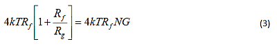
In this form of the output-noise equation, the two resistor-noise terms combine into a single element: 4kTRfNG. Equation 2 shows the two noise power terms separately, while Equation 3pulls 4kTRf out of that sum and collapses it to the last term under the radical in Equation 1.
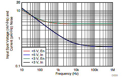
The spot noise of each FDA input-noise term increases as the frequency decreases. You can see this 1/f effect in the input spot-noise plot for the Texas Instruments THS4551 [2], as shown in Figure 2.
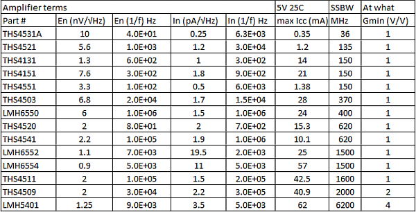
The goal of this analysis is to predict the integrated noise for DC-coupled channels through a defined noise power bandwidth (NPB) and combine that with an ADC’s reported signal-to-noise ratio (SNR) to predict the SNR degradation adding to the input FDA stage. The FDA terms required for this analysis are the flat-band voltage and current spot-noise values, and approximate 1/f frequencies. Table 2 summarizes the required terms for a range of modern FDA devices.
One way to include the effect of increasing spot noise at low frequencies is to generate an integrated noise power up through the expected NPB and then substitute an equivalent flat-noise value over frequency to plug into Equation 1. This value will integrate to the same power as an ideal 1/f spectral shape.
Most designs will define an NPB using a passive filter between the output of the FDA to the input of the ADC. For an initial design check, you can use this filter’s NPB to estimate the equivalent flat noise that will include the 1/f effects. Using an arbitrarily low-frequency start to integration (usually 0.1Hz) as F1, Equation 4 shows the simple adjustment to the amplifier’s flatband value to include the 1/f effect [4]. Here, F2 is the expected NPB and F3dB is the 1/f corner frequency from Table 2. Equation 4 shows this calculation using voltage noise, but the method is identical for current noise.
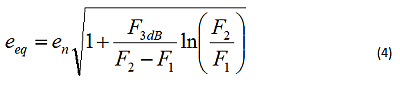
When the NPB is far greater than the 1/f corner frequencies, Equation 4 will make only a very small adjustment to the flatband value for use in Equation 1.
A critical step in the definition of new FDA devices is to balance the noise terms in the nominal design recommendations. Balancing terms shows up as a suggested feedback-resistor value at the nominal specification gain. This critical starting-point value for Rf also influences the total power in the solution and the phase shift back to the summing junctions in the loop-gain phase-margin analysis [1, section 8.2].
Next: Combining an FDA with an 18-bit SAR ADC and predicting combined SNR performance