


Confirming SNR estimates using simulation tools
The design calculations shown here give you a quick way to compare solutions and identify the key terms in an FDA design that drives a high-precision ADC. The calculated values are reasonably accurate for a simple interstage RC filter. However, most designs are more complicated, with feedback capacitors or active filter implementations in the FDA stage. Those cases will require using simulation to get a more accurate view of the SNR to the ADC input pins.
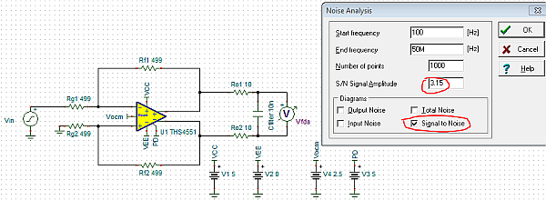
Continuing with the lowest-noise case shown in Table 9 with the THS4551 and 499Ω resistors, you can perform an SNR simulation using a free SPICE-based simulator such as TINA-TI™ software. When setting up the SNR conditions, enter the maximum RMS voltage level you would be comparing to in simulation. Here, that level would be the 3.15Vrms corresponding to the 8.9Vpp test level used in reference [5].
The simulation is running a swept integration of noise and delivers a curve of SNR up through the maximum 50MHz shown in Figure 4. This 50MHz end value includes the full NPB of the 30MHz input signal bandwidth for the ADS8881 [6]. Figure 5 shows this simulation and the final full bandwidth SNR delivered to the ADC inputs of 110dB.


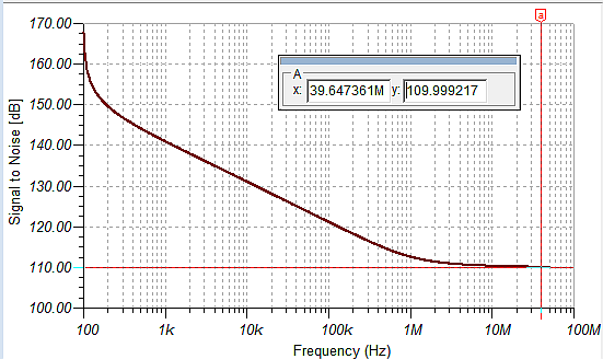
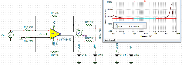
This simulation result is slightly worse than the predicted level of 110.25dB in Table 9. One possibility for the discrepancy might be that this design is showing some higher-frequency output spot-noise peaking not included in the simplified analysis. RC loads often reduce the phase margin in modern high-speed FDAs like the THS4551 (simulations showed a 27-degree phase margin in this example). Running an output spot-noise simulation at the FDA output pins as shown in Figure 6 easily confirms this. Here, the low-frequency 1/f effects included in the model are visible, and indeed some spot-noise peaking appears at the unity loop-gain crossover around 32MHz. The marker at the midband shows the 8.75nV/Hz spot noise predicted in Table 9for this design. The post-RC interstage filter effectively attenuates this peaking in FDA output spot noise. But the simulation does integrate to very slightly reduce the SNR to 110dB, compared to the expected 110.25dB from the simplified analysis (assuming a flat output-noise spectrum above the 1/f corners).
Conclusion
While many treatments of FDA output-noise analysis exist, most neglect the 1/f effects that are easy to include in the analysis as shown here. Breaking out the separate terms at the output will clearly show where you can make the most impact, either by changing the FDA or the resistor values.
SNR calculations are simple, but must have a defined bandwidth for definition, which is usually provided by an interstage passive filter to the ADC. This passive filter provides many other useful functions, but one is to set the integration bandwidth for the spot noise out of the FDA.
Designs often include more involved passive or active filters. Starting with the simplified flow shown here will help you move in the right direction toward an initial design, where you can then use full circuit simulation for final SNR estimates. Using the simulated SNR (it is critical that the model accurately includes the noise and phase-margin effects) in Equation 6 will give you a preview of combined SNR before physical testing.
Often, the filtering around the FDA will reduce the phase margin. If peaking is visible, check the phase margin and perform a quick simulation of the spot output noise across the FDA output pins, which is a good indicator of low phase margin.
About the author
Michael Steffes has participated in the development and introduction of >80 high-speed amplifier products since 1985. He has previously published >25 app notes and >55 original articles covering a variety of high-speed amplifier issues and applications. He currently works as a Senior Member of Technical staff in the definition and development of industry leading signal path components supporting precision and high-speed data converters for Texas Instruments.
References
- THS4541 Negative Rail Input, Rail-to-Rail Output, Precision, 850-MHz Fully Differential Amplifier, Section 8.5
- THS4551 Low-Noise, Precision, 150-MHz, Fully Differential Amplifier, Section 10.1.1
- Fully Differential Amplifiers, James Karki, Texas Instruments, September 2016
- Noise Analysis for High-Speed Op Amps, Michael Steffes, Texas Instruments, January 2005
- 18-Bit, 1MSPS Data Acquisition Block (DAQ) Optimized for Lowest Distortion and Noise, Vaibhav Kumar, Texas Instruments, October 2015
- ADS8881x 18-Bit, 1-MSPS, Serial Interface, microPower, Miniature, True-Differential Input, SAR Analog-to-Digital Converter