


Combining an FDA with an 18-bit SAR ADC and predicting combined SNR performance
To illustrate FDA noise analysis, consider the relatively simple 18-Bit, 1MSPS Data Acquisition Block (DAQ) Optimized for Lowest Distortion and Noise precision design from Texas Instruments [5] using the THS4521 FDA to drive the ADS8881 ADC (Figure 3). This circuit has a simple gain of one stage using 1kΩ resistors and a single-pole resistor-capacitor (RC) interstage filter to the ADC. The requirements of the ADC often dictate the selection of this RC filter.


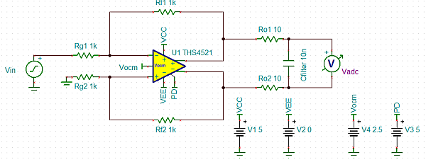
This example RC filter between the FDA outputs and the ADC inputs sets an NPB of:
1.57*(1/(2π*10*20nF)) = 1.22MHz
Note that the differential C is doubled on each side to set the pole.
The tested output swing into the ADC is 8.9Vpp (3.15Vrms) in reference [5]. To compute the integrated noise through the NPB, you will need to develop each of the terms in Equation 1.
Pulling the noise terms for the THS4521 from Table 2 and using the NPB=1.22Mhz=F2 in Equation 4 provides the very slight adjustments necessary in this case for the FDA noise terms to account for the 1/f low-frequency noise effects. Table 3 summarizes the FDA input noise adjustments using Equation 4.
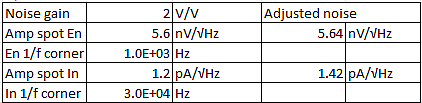
In this example, the NPB is high enough that the voltage noise flatband dominates the integrated noise, while the current noise gets a very slight adjustment. It is important to include this effect, as different combinations of noise terms and NPB might include a more significant 1/f contribution. For instance, calculating Table 3 for a 400kHz NPB = F2 in the RC following the THS4521 in Figure 3 provides updated equivalent spot-noise terms to use in Equation 1. This is summarized in Table 4.
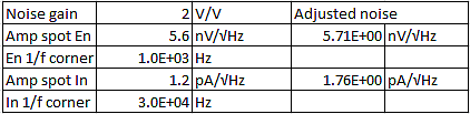
Here, you’ll see more adjustment in the required flat spot noise to use in Equation 1 to account for the 1/f effects in the FDA input-noise terms. In both cases, Equation 4 used a starting frequency (F1) of 0.1Hz.
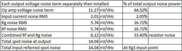
Using the adjusted terms in Table 3, each of the terms in Equation 1 computers to the output spot-noise voltage contribution shown in Table 5 (taking the square root of each of the power terms in Equation 1). Table 5 shows the two resistor-noise terms separately first, then combined as in Equation 1. Notice here that the FDA voltage-noise contribution is dominant – reducing the resistor values will have little effect on this design toward reducing the total output noise.
Using 14.04nV/√Hz differential spot noise at the FDA outputs, and the 1.22MHz NPB of the interstage filter, you can calculate the root-mean-square (RMS) noise and SNR at the ADC input pins. Typically, the resistors in the interstage filters are low enough to add only negligible amounts to the total noise delivered; you can neglect their contribution for total noise purposes.
The RMS noise delivered at the output of the RC filter will be this spot-noise voltage multiplied by the √NBP. Table 6 shows the results of these calculations.
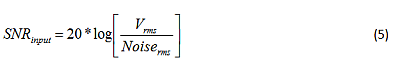
Once you have calculated the integrated noise (15.5µVrms in this case), you can usually calculate Vpp noise using a 6x crest factor on the RMS noise (93µVpp in this case). Using the intended maximum RMS signal level (3.15Vrms in this case) and the RMS noise delivered, Equation 5 calculates the SNR to the ADC inputs caused by the FDA-plus-RC filter stage.
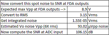
The example design in reference [5] used a 4.5V reference (9Vpp absolute maximum differential input range) and entailed testing with 8.9Vpp maximum at the FDA outputs. With this 106.15dB SNR estimate at full scale delivered to the ADC input pins, Equation 6 calculates a combined SNR with the reported ADC SNR. Putting the 99.5dB reported as typical for the ADS8881 ADC at the 10kHz input frequency used in references [5] and [6], and using the 106.15dB for the THS4521 FDA interface of Figure 1 into Equation 6 gives a combined SNR = 98.65dB.
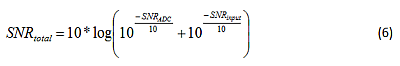
Table 7 shows the combined measurements from reference [5]. Using the actual 4.5V reference column, the FDA plus RC filter plus ADC shows a 98.73dB combined result, very closely matching the expected 98.65dB result.
After developing this methodology, it’s now an easy matter to try different FDA solutions and quickly observe the impact on final SNR. Referencing the FDA selections available in Table 2, the THS4551 FDA is a lower-noise upgrade to the THS4521, with similar power and speed. Using the THS4551 noise specifications, you can calculate a comparative total SNR value for the same configuration. Table 8 compares intermediate results and final SNR reduction showing the improvement in total SNR using this lower-input voltage-noise FDA.

In both cases listed in, the current noise contributes very little to the total output noise. For the THS4521, the FDA voltage noise is dominant, so you can expect little improvement by reducing the resistor values. Using exactly the same configuration with the THS4551 will reduce SNR losses from 0.77dB to only 0.44dB. However, because the resistor-noise terms in the second solution are dominant, reducing those values will further improve SNR at the cost of more power in the feedback networks. Using 499Ω R values in the THS4551 solution changes the comparison to that shown in Table 9 – another 0.13dB improvement in combined SNR.

Next: Confirming SNR estimates using simulation tools