


EMI compliance is becoming a major concern for advanced power electronics due to increasing switching speeds. Correlated time-frequency measurements help optimize gate driving and minimize electromagnetic emission already during development.
 Task
Task


The use of wide-bandgap materials such as silicon carbide (SiC) and gallium nitride (GaN) enables high switching frequencies and steep rising edges, as well as high voltages. These characteristics enhance the efficiency of switching power supplies and increase the challenge to meet EMI compliance. Taking design guidelines for reduced EMI into account is just as important as testing and optimizing for EMI compliance in the development phase.
Rohde & Schwarz solution
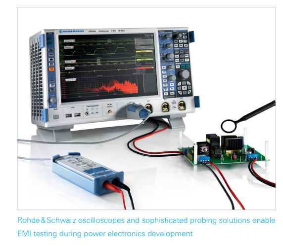
Oscilloscopes are powerful tools that support everyday tasks of electrical engineers. The sensitivity and performance of today’s oscilloscopes enable EMI optimization tasks during the design phase of a new product. Direct frequency and resolution bandwidth input and a fast update rate are useful features of Rohde&Schwarz oscilloscopes. In combination with the R&S HZ-15 compact probe set for E and H near-field measurements and the R&S HZ-17 compact H near-field probe set (both with 3 GHz bandwidth), the source and transmission path of unwanted emissions on a PCB can be easily located.
Application
Gated FFT for correlated time-frequency analysis
For advanced analysis, e.g. correlation between time and frequency domain signals, the gated FFT functionality of the R&S RTE1000 and R&S RTO2000 oscilloscopes is essential. This function restricts the spectrum analysis to a user-defined region of the captured time domain signal.
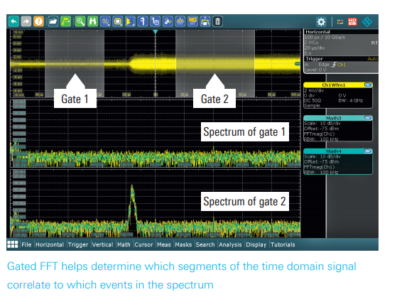 Excessive spectral emissions can thus be correlated to dedicated time periods in a continuous signal. During EMI testing, this not only helps identify the source of unwanted electromagnetic emissions in time domain signals, it also enables straightforward testing of different operating scenarios.
Optimizing gate driving voltages with respect to EMI emission
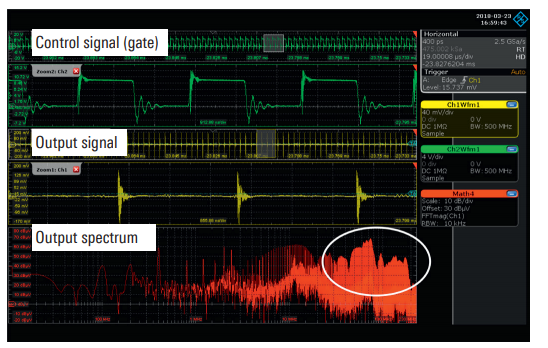
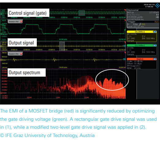
One source of EMI emissions in power electronics circuits is the fast-switching MOSFET bridge. Modifying the gate driving voltage of the switching transistors is a straightforward possibility to reduce EMI. This requires parallel measurement of the gate driving voltage, the output signal and the emitted radiation, as well as their spectrum.
In the figure below, various drive signals of a MOSFET bridge and their effect on the emitted radiation is analyzed. In (1) a rectangular gate drive signal was applied, whereas in (2) a cascaded two-level rectangular gate drive signal was used (green). Parallel monitoring of the EMI emission with a near-field probe clearly shows that this is an effective method: the amplitude of the high-frequency components in the EMI signal (red) is reduced effectively.
 Further optimization steps
To determine the optimal gate drive voltage, additional parameters have to be analyzed. Switching loss is an important criterion and might increase with changed gate drive signals. For switching loss measurements, current probes and high-voltage differential probes are necessary, and their maximum voltage and current as well as their bandwidth are crucial. Current and voltage signals have to be deskewed to avoid measurement errors of the switching loss:
- R&S RT-ZHD high-voltage differential probes are ideally suited for fast-switching semiconductors. They support up to 200 MHz bandwidth and maximum measurable voltages between 750 V and 6 kV, combined with a high common-mode rejection ratio.
- R&S RT-ZC current probes allow current measurements between 5 A (RMS) with a bandwidth of 2 MHz and 500 A (RMS) with a bandwidth of 120 MHz.
- R&S RT-ZF20 power deskew and calibration test fixtures compensate the different delay between current and voltage probes. This is essential to accurately measure the switching loss.
Summary
The fast and flexible FFT function of Rohde&Schwarz oscilloscopes supports detailed EMI testing for power electronics already in the development phase of state-of-the-art electronic devices. In combination with near-field probes and high-voltage differential or current probes, full optimization of power electronic circuits is possible without the necessity of additional test tools. This speeds up power electronics development during the device design phase and helps to pass EMC qualification testing.
Article Courtesy: Renesas Electronics