


Abstract
As we push through lower technology nodes in the IC and chip design, the wire width goes thinner along with transistor size. This makes the wire resistance more dominant on 16nm and below technology nodes. This increasing resistance and the decreasing width of metal wires introduce many Electromigration and IR drop issues. These two issues play major roles in reducing the lifespan of an electronic device and are the causes of functionality failure in any electronic devices with lower technology nodes.


In this article, we will discuss the problems of electromigration and IR drop, and techniques to prevent the occurrence of these issues in electronic devices.
Technology Trends Impacting Nanometer Sizes:
The technology trends and demand for compact electronic devices require modern IC designs. Electronic equipment manufacturers are exponentially decreasing the metal interconnect width. As a result, the cross-sectional area of interconnect is shrinking. Moreover, due to the increasing functionality integration and devices interconnection, there are more wires on a die. Hence, any device working on nodes lesser than 16nm is susceptible to performance issues over a period, due to the failure of passing proportionate currents, leading to issues of electromigration and IR drop.
What is Electromigration?
Electromigration (EM) is a molecular displacement due to the momentum transfer between conducting electrons and ions over a period of time. It occurs when the density of the current is high, which causes the metal ions to drift in the direction of electron flow. EM usually occurs after years of deployment of devices in the field.
Due to electromigration effects, the metal wires may burst into open and shorts. EM can increase wire resistance, which can cause a voltage drop resulting in device slowdown. It can also cause permanent failure in circuits due to shorts or opens. EM goes in a positive feedback loop with temperature (Joule Heating). Here is how to find the Mean Time to Failure (MTTF) of a metal line with Black’s Equation.
Electromigration reliability of a wire (Black’s equation)
A = Cross-section area dependent constant
Jn = Current density
Ea = Activation energy k = Boltzmann’s constant T = Temperature in kelvins
N = Scaling factor (usually set to 2 according to Black)
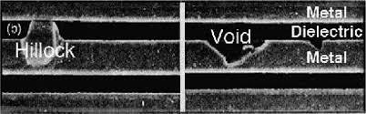
What is IR Drop?
IR drop is the voltage drop in the metal wires constituting the power grid before it reaches the power pins of the standard cells. It becomes very important to limit the IR drop as it affects the speed of the cells and overall performance of the chip. There are two types of IR drops:
- Static
- Dynamic
Static IR Drop:
Static IR drop is an average voltage drop for the design. It is dependent on the RC of the power grid connecting the power supply to the respective standard cells. The average current depends totally on the time period. Gate-channel leakage current is the major reason for the static IR drop.
Vstatic_drop = Iavg x Rwire [Iavg are all factors of leakage currents ]
Dynamic IR Drop:
Dynamic IR drop is a drop in the voltage due to the high switching activity of transistors. It happens when there is an increasing demand for current from the power supply due to switching activities of the chip. Dynamic IR drop depends on the switching time of the logic and is less dependent on the clock period. Dynamic IR drop evaluates the IR drop caused when a large number of circuitry switches at the same time, causing peak current demand. This current demand could be highly localized and could be brief within a single clock cycle (a few hundred ps), and could result in an IR drop that causes additional setup or hold-time violations. Typically, high IR drop impact on clock networks causes hold-time violations, while IR drop on data path signal nets causes setup-time violations. In such cases, you can separate the standard cells apart so that the burden on a given bump to feed many standard cells, which have high switching activity, can be mitigated.
Vdynamic_drop = L (di/dt) [current L is due to switching current]
A Case in Point:
EM violations in networking ASIC in 16nm FF+
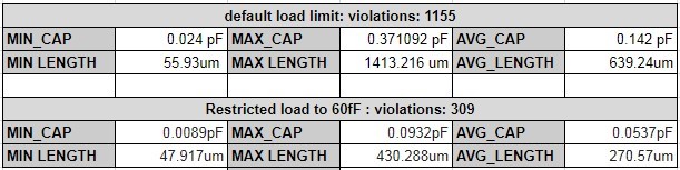
We observed 1155 electromigration violations on signal/clock nets. We had max_cap of 371fF load and average net length was ~640um. Capacitance load was based on the default value in the standard cell lib. This enabled nets to allow more current.
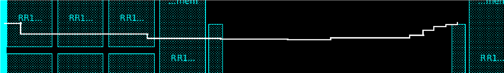 Total capacitance of APSDRC_net_210033: 0.34327 Total length of APSDRC_net_210033: 1345.995
IR challenges in networking ASIC in 16nm FF+
We saw an IR drop around clock cells since they were always switching with a duty cycle of 50%. We observed that there were standard cells in close proximity of clock cells through which the overall area got very denser. Because of this, there was an IR drop around such areas.
Apart from the clock, we saw an IR drop hotspot on some of the power-hungry cells and highly dense region.
Techniques to prevent Electromigration and IR Drop
Electromigration Mitigation
- Apply NDR (Non-default Rule) on the violated nets (vulnerable nets)
Once you have the EM results, you can take the net shapes and re-route those nets with the NDR. Applying NDR involves routing of clock nets using double-wide or triple-wide metal with more spacing. This will quickly remove most of the violations and can even predict the nets, which are more likely to have EM violation based on two parameters: 1) driver strength and 2) load.
You can filter out nets with more load and heavy drivers and move them to NDR. You can decide the threshold load for different driving strength based on project statistics.
Example: We saw an amazing improvement on one of the blocks
Command: create_routing_rule em_ndr -widths “M2 0.064 M3 0.064 M4 0.064” -cuts {{VIA1 {Vrh 1} {Vrv
1}} {VIA2 {Vrh 1} {Vrv 1}} {VIA3 {Vrh 1} {Vrv 1}} {VIA4 {Vr 1}}}
foreach net [gon [get_nets $nets] ] { set_routing_rule $net -rule em_ndr }
 Before these settings, there were 309 violations, which reduced to 1 after applying NDRs.
2. Restricting load target for nets
Restricting or reducing the load on the nets can also be helpful in preventing the occurrence of electromigration. In the above example, we saw 142fF as an average capacitance in the design. Based on the statistics of a few experiments, we restricted all nets to have a maximum 60fF of load. As a result, we saw a very good improvement in signal EM as well as on average net length.
Command: set_max_capacitance 0.06 [current_design] #setting max_cap_value for the design
IR Drop Mitigation
- Padding clock cells
When it comes to IR drop issues, clock structure is the primary culprit for the power consumption of the chip due to high clock switching. However, with padding clock cells technique, clock buffers/inverters and clock gate cells are given extra area as keepout regions to avoid placement of standard cells and any excessive cell density around them. This helps to prevent the dynamic IR drop.
Command: create_keepout_margin -outer {3.6 0.576 3.6 0.576} $clock_type_keepout IMAGE: A cell with cell padding
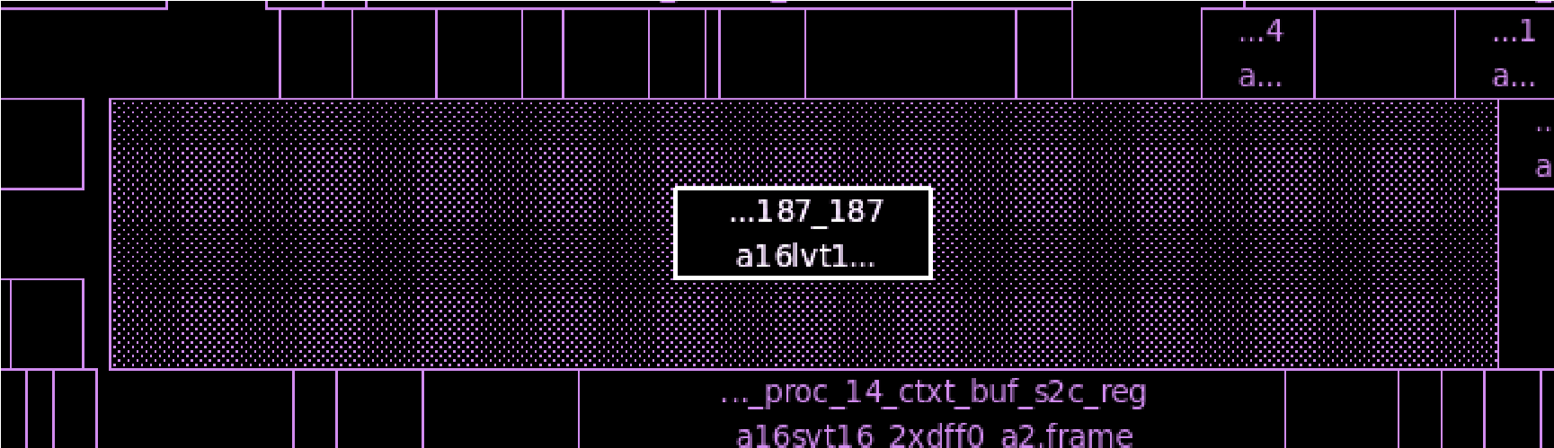 2. Cell Padding/Decap insertion around cells within a dynamic IR hotspot region
Some cells with high driving strength create dynamic IR drop issue. You can give cell padding to these cells or insert decap cells around it or IR hotspot region to prevent IR drop issues.
Conclusion:
When it comes to lower geometry designs, the issues of IR drop and electromigration are common. With techniques like padding on clock cells, restricting maximum load on nets and applying NDR on clock nets, you can prevent major IR drop issues and reduce electromigration in lower geometry chip designs.