


There are many challenges in circuit design today and understanding the key differences between digital isolators and opto-coupled isolators in circuit design helps developers design more effectively. This whitepaper reviews the challenges of modern circuit design, industry design trends, the use of various isolators, such as CMOS digital isolators, and the benefits of each.
The design of modern electronic systems in applications are as varied as industrial automation, power supplies for telecom base stations, and on-board chargers (OBC) for electric vehicles (EV) and comes with a unique set of challenges:


- Providing safety from high voltages – for electronic control equipment as well as human operators
- Effective communication across sub-systems with relatively high ground potential differences
- Preventing electrical noise from corrupting sensitive signals
These challenges can be solved by introducing galvanic isolators in the circuit design. Galvanic isolators are devices that couple an electrical data or control signal across an insulation barrier without any flow of current through it, thereby enabling signals to be transferred while blocking noise. The insulation barrier also safeguards equipment and human operators from high voltages.
Opto-coupled isolators
The earliest isolators were optically-coupled devices, also called opto-isolators or optocouplers, “optos” for short. The first patents for optos were issued in the 1960s. Earliest forms consisted of miniature incandescent light-emitting bulbs on the primary side, a clear (optically transparent) plastic, which acted as the insulation or dielectric layer as well as the optical path, and a photo-resistor on the secondary side, whose resistance was modulated by the amount of light falling on it. Later developments introduced more sophisticated opto-coupled devices that made the system designer’s job a little easier. They were all basically some sort of light-emitting structure (the miniature bulbs were replaced by a semiconductor-based light emitting diode or LED) on the primary side, coupled with various forms of light-sensitive devices such as a photo-resistor, photo-transistor, photo-diode or triac that made the device suitable for a range of dc and ac applications. Optos were basically the only solution available until CMOS-based digital isolators were developed in the late 1990s using inductive (magnetic) or capacitive coupling to transfer the signal.
Figure 1 highlights the technology differences between opto-couplers and digital isolators.
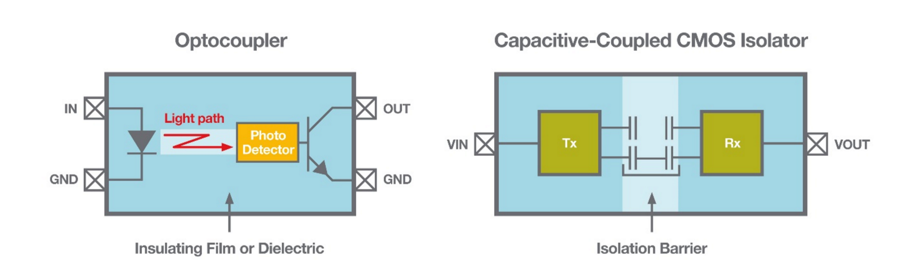
Figure 1. Basic operation of opto vs capacitive coupled CMOS isolator
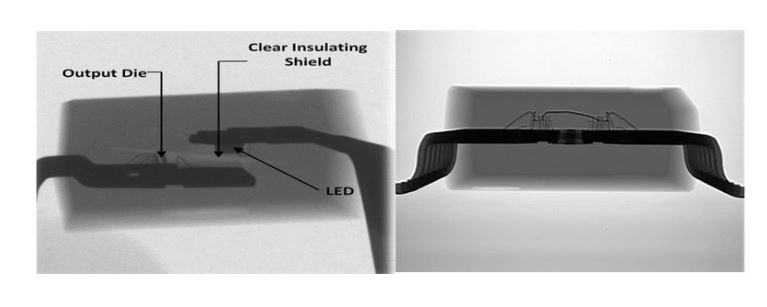
Figure 2 shows examples of X-ray images of an opto-coupler assembly (left) and a digital isolator assembly (right) to help visualize the physical construction of these devices.
 A prominent characteristic of the opto is the aging problem. The quantum efficiency of the LED, defined as the total photons per electron of input current, decreases with time at a constant current. This is largely due to the electrical and thermal stressing of the PN junction. This had implications for the optocoupler’s long-term stability and operation, especially at high temperature operation. The designer can compensate for aging by doing several things:
- Decrease real operating life
- Decrease operating diode current and ambient temperature
- Avoid peak transient currents.
Of course, these actions put limitations on the use case, since isolators are most useful in systems where such conditions exist intrinsically. Digital isolators have no such physical limitations. Since optos basically function by switching the PN junction diode, they have a relatively slow switching rate. Therefore, optos are only capable of lower data rates with large propagation delays and skew.
Industry Trends and CMOS Digital Isolators
In an increasingly bandwidth and power-hungry world, new CMOS-based digital isolators provide an ideal solution. The most common applications for isolation are in the industrial market – in equipment such as factory automation, process control, programmable logic controllers (PLC) or process automation controllers (PAC), inverters for motor control and uninterruptable power supplies (UPS). Industrial automation is the largest market for isolators, and designers of industrial systems value the high-temperature operation, superior part-to-part matching, low skew and high noise immunity that CMOS isolators bring to the table.
Other heavy-use applications include isolated power supplies used in telecom base stations and in servers that power the infrastructure behind our increasingly connected world – the Internet of Things. The early adopters of digital technology were isolated power supply manufacturers. These power supplies were primarily used for servers and telecom base stations. For this market, the most critical parameter was power density, and the mantra was W/mm3. It helped that worldwide green initiatives for a cleaner environment also mandated higher efficiency to reduce wasted energy. As it turns out, having a higher efficiency system also implies less heat loss, which leads to further reductions in system size because space-consuming heat sinks were no longer required. The biggest impact of CMOS digital isolator technology was on the timing characteristics of these new isolator devices compared to optos.
Since these were not based on switching the PN junction of the LED for enabling signal transfer, the switching rates improved by an order of magnitude. Combined with the advantages offered by the smaller geometries and the more repeatable and stable manufacturing process used by standard CMOS silicon technology, timing parameters such as propagation delays, pulse width distortion or skew, part-to-part matching and common mode transient immunity (CMTI) were vastly improved. In the isolation industry, CMTI basically refers to common mode noise rejection capability, measured as a voltage slew rate, kV/µs. The limitations of optos were due to the manufacturing process involving compound semiconductor technology, which is better suited for optical operation rather than for fast and accurate devices. The inherent advantages of digital isolators helped power supply OEMs tighten up the power converter control loop timing, thereby gaining efficiency.
Another fast-emerging market for digital isolators is automotive. Whereas traditional internal combustion engine (ICE) based automobiles hardly used any isolators, this has changed since the introduction of electric vehicles (EVs). EVs or the various forms of hybrid electric vehicles (HEVs) have a high-voltage battery ranging from 200V to 400V today, and higher voltages are planned in the future to enable higher power and/or capacity for maximizing the distance per charge. This high-voltage battery necessitates the use of isolators for safety and signal transfer across different voltage domains within the vehicle. Virtually all major automobile manufacturers have an imminent EV/HEV rollout plan. The automotive industry is also proving to be an early adopter of digital isolator technology due to its superior high temperature operation, stability and noise immunity. End applications such as battery management systems (BMS) and chargers are driving the need for isolators in the EV/HEV market.
Optos still enjoy the majority share of the overall isolation market
Optos still enjoy the majority share of the overall isolation market, even within the high-performance sector (roughly characterized as isolator products with data rates of least 1 Mbps and specialized products such as gate drivers). Despite the intrinsic performance shortfalls of optos, they still have a few advantages in the market. The biggest advantage is that optos have been the de-facto solution for decades; designers are comfortable with using optos and feel they are safer – after all, isolators are safety devices.
Digital isolators have come a long way from the earliest implementations, which typically only provided a basic insulation level (roughly translating to a 2.5 kV isolation rating). Today, digital isolators are available in reinforced and double insulation ratings (5 kV or more) and are deemed to be on par with optos for providing safety. The other advantage of optos is that they are intrinsically immune to external electro-magnetic (EM) fields and also radiate less EM noise. This is a plus in industrial markets where generators of high EM fields, such as heavy-duty induction motors, exist on the factory floor, for example, and electronic systems need to be tolerant of such external fields. Capacitive-based digital isolators are also highly immune to external EM fields and radiate low levels compared to the magnetic based digital isolators. In general, though, digital isolators are superior in terms of timing characteristics, stability over lifetime, CMTI and high temperature operation. Table 1 provides a summary explanation of the advantages and disadvantages of optos and CMOS digital isolators.
The growth rate of digital isolator products is roughly twice that of the overall isolation market
The growth rate of the digital isolator products is roughly twice that of the overall isolation market, which shows the increasing confidence among end users to switch their designs from the traditional optos to digital isolators.
| Item | Impact | Digital Isolators | Optocoupler |
| Timing performance | Enables higher throughput and efficiency for end product | Low propagation delay and skew, better part to part matching | High propagation delays and skew, worse part to part matching |
| Parasitic capacitive coupling | The lower the parasitics, the higher the CMTI | Less than half the parasitic coupling of optocouplers | High parasitic coupling with interdependent parameters |
| Reliability and high temperature operation | Longer product lifetimes | No wear out mechanisms, 60+ year operating lifetime at 125
°C at maximum VDD |
Intrinsic wear-out mechanisms; 10x lower lifetime |
| Input current | High input current means higher power consumption | CMOS input buffers need very low input current | Requires higher input current to be competitive |
| Ease-of-use | Minimum external BOM needed to extract full functionality and
performance |
Fewer second order effects, minimum BOM required for full performance guarantee | Significant first and second order effects, temperature dependencies, imprecise current thresholds, CTR require external
BOM to get stable performance |
| Electro-magnetic immunity and radiation | Immunity provides robustness and low radiation implies low noise generation | Capacitive-coupled devices are comparable to optos while magnetically coupled devices can be noisy and are susceptible to external EM noise | Optos are generally highly immune and have low radiation |
| Safety compliance | Ensures safety standards are tested and certified | General trend is newgeneration isolators are on par with optos | Optos have traditionally been used for many years and are compliant |
Table 1: Comparison of optocouplers and digital isolators.
Compliance and Safety Standards
Isolation safety standards play an important role in assuring the end user that the isolation solution they have chosen has been tested to universal standards and has been found to perform satisfactorily. In this regard, digital isolator manufacturers and opto manufacturers recognize that the final beneficiary is the end user and therefore have cooperated in defining a new compliance standard that is not merely a hand-me-down opto standard but one that genuinely accommodates the manufacturing and design differences between an optocoupler and CMOS digital isolator. This new VDE 0884-11 standard is already a valid specification. Furthermore, the IEC 60747-17, a soon-tobe-published IEC version of the standard, will go a long way in allaying customer concerns.
Conclusion
CMOS-based digital isolators make full use of state-of-the-art semiconductor technology and offer several key advantages to the system designer over traditional optos. As we have seen, these advantages are game-changing and have helped shape the evolution of industries such as power supplies, green energy and automotive and will continue to drive innovation in other markets in the near future.
Article Courtesy: www.silabs.com