


Efficient signal acquisition is fundamental to applications ranging from industrial process control and measurement to high-speed communications and imaging. Across this broad range of applications the ability to match the proper component to the task is essential for creating a signal chain fully able to meet performance requirements at the lowest possible cost. This balance of cost and performance becomes even more important with the expected proliferation of deeply embedded sensor systems feeding the Internet of Things (IoT). With IoT device counts expected to number in the tens of billions, savings achieved at each stage of the signal chain translates into significant savings overall.
For designers, building an effective signal chain means balancing specifications of individual components within each stage to meet target performance levels of the signal chain as a whole. While some applications require devices with the highest possible specifications (Figure 1), designers can often use more cost-effective components that nevertheless complete a signal chain with the required level of performance and functionality.


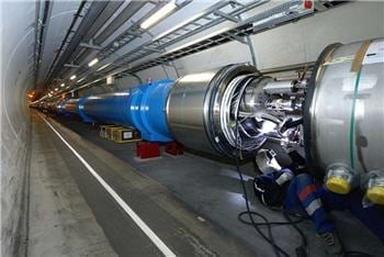
Figure 1: High-performance analog components including analog-digital converters and multiplexers enable CERN’s Large Hadron Collider to measure magnetic fields with the highest performance possible.
In its most basic form, a signal acquisition circuit would ideally comprise only one component: an analog-digital converter (ADC) to digitize analog input signals from sensors or other sources. For any practical application, however, the realities of real-world signal characteristics preclude such a simple approach and drive further requirements for signal conditioning including amplification and filtering (Figure 2). For applications using active sensors, additional components, such as digital-analog converters (DAC), precision voltage references and amplifiers are needed on the front end to provide sensors with required excitation current or voltage levels.
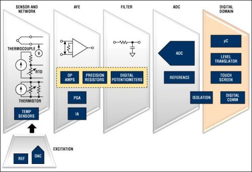
Figure 2: Prior to data conversion, a typical analog signal chain requires conditioning to compensate for small-signal inputs, signal offsets, and other signal characteristics unique to each application. (Source: Maxim Integrated)
Signal Conditioning
Typically, sensors and transducers produce small-amplitude signals. Without amplification, these signals would allow use of only a portion of the full dynamic range of an ADC, most likely resulting in loss of fine detail due to limited ADC resolution and heightened impact of converter quantization on error. Consequently, designers typically need an analog front-end (AFE) amplifier stage to increase the span of the input signal to match the full dynamic range of the ADC. Just as important, an input amplifier can ensure sensors and transducers remain properly loaded, while also buffering the front end from load transients found on the inputs of some types of ADCs while signal sampling.
Engineers can find amplifiers across a broad range of features and performance capability. Although the natural tendency is to find an amplifier with the highest possible performance specifications, engineers can dramatically reduce the cost of their designs by rigorously comparing amplifier specifications to the characteristics of the input signal and the required resolution of the output. For example, an instrumentation amplifier (IA) with the fastest possible slew rate and lowest possible noise might simply add unnecessary expense when the signals of interest change at a slow rate and remain well above the noise floor. Similarly, an amplifier with the best possible linearity specifications could simply outperform an ADC that delivers results with sufficient accuracy while nevertheless exhibiting quantization error at levels that are significant, yet well within overall performance requirements for the signal chain.
Based on signal characteristics and application demands, engineers facing more stringent requirements can choose a variety of full-featured amplifiers, such as high-precision IAs, low-noise amplifiers (LNA), and programmable gain amplifiers (PGA). Still, conventional op amps provide performance characteristics suitable for most applications. For example, rail-to-rail-input/output (RRIO) low-noise op amps such as Analog Device’s AD850x, Maxim Integrated’s MAX963x and Texas Instruments’ OPA320 series provide a low-cost option able to maximize the dynamic range and minimize noise in a broad range of signal-acquisition applications.
Although conventional single-ended input amplifiers are sufficient for many applications, differential inputs are required for many signal acquisition applications where good common-mode rejection is a key requirement. For example, applications using bridge sensors or designs operating in very noisy environments require high-common-mode rejection characteristics available with amplifiers with fully differential inputs. In fact, some differential amplifiers such as Analog Device’s AD8476 and Texas Instruments’ THS4531 are designed specifically to address differential signal-conditioning requirements and include features designed to simplify the interface to ADCs. Along with ADC interface options, features such as integrated laser-trimmed resistors found in Analog Device’s AD8476 help reduce component count and cost in signal chain designs (Figure 3).
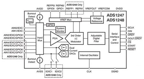
Figure 3: Differential amplifiers such as Analog Device’s AD8476 feature integrated laser-trimmed resistors and output capabilities tuned to ADC interface requirements help simplify design of signal chains with differential input requirements.
While amplification extends the span of input signals, it also exacerbates signal noise characteristics that effectively limit dynamic range. As a result, signal chains typically require a filter stage prior to conversion to limit the impact of noise at frequencies outside the signal of interest.
For applications requiring maximum flexibility, engineers can build these filters using digital potentiometers such as Maxim Integrated’s MAX540x and Texas Instruments’ TPL0102 series and drive them with simple control logic or through the host MCU. For applications with relatively stable signal characteristics, however, simple passive components can often meet the design’s filtering requirements.
Beyond noise-bandwidth limitation concerns, signal chains have typically required use of an anti-aliasing filter to reduce sampling artifacts at frequencies above half the sampling rate. The availability of oversampling conversion methods has greatly reduced the need for this stage.
Signal Conversion
Signal conditioning circuits comprising amplifiers and filters are designed for the sole purpose of delivering a clean signal to the input of an ADC. Consequently, the complexity and performance specifications for those front-end components derive largely from the characteristics and requirements of the ADC. A costly high-precision amplifier is an unnecessary expense in a signal chain required only to provide relatively low-resolution conversion of slow-changing signals.
In practice, the choice of the most suitable ADC – and therefore the choice of the required signal conditioning components – derive in turn from careful analysis of the characteristics of the input signals and overall functional requirements of the application. The precision (and cost) of a signal chain for an application that periodically measures gradual changes in ambient temperature will be far different from one intended to provide instantaneous feedback in a mission-critical process-control application. Indeed, ADC selection is typically driven by requirements for signal conversion throughput and latency time (the time between the beginning of signal acquisition and the time when the ADC makes the corresponding data available on its outputs).
Engineers can draw from ADC architectures designed to deliver dramatically different levels of performance. Each architecture provides inherent capabilities and limitations for achieving high throughput and low latency. For example, flash ADC architectures typically offer the highest throughput and lowest latency but are generally cost-effective only at lower-bit resolutions. Flash ADCs, such as Analog Device’s AD782x and Texas Instruments’ TLC0820, use a parallel configuration of conversion elements to perform high-speed conversion. Their high throughput and minimum latency make them ideal for voice encoding applications, for example, where significant latency cannot be tolerated.
In contrast, successive-approximation-register (SAR) and sigma-delta (ΣΔ) ADCs provide cost-effective performance across a wide range of requirements and applications. SAR ADCs have emerged as the predominant choice for most medium- to high-resolution applications. These devices complete conversion in a single cycle, making them suitable for data-acquisition applications requiring minimum latency time, such as control loops, power monitoring, and signal analysis.
ΣΔ ADCs generally offer the lowest cost option for high-resolution conversion due to their inherent oversampling architecture. On the other hand, relatively slow settling time and sharp cutoff of internal digital filters in conventional ΣΔ ADCs have limited their use in some applications. As a result, designers have sometimes opted for a SAR ADC even in situations where the performance of a ΣΔ ADC would be adequate. For example, SAR ADCs have traditionally been the first choice for use in control loops and multiplexed applications because of concerns over the performance of conventional ΣΔ converters.
Feedback delays can create instability in control loops for an industrial process, household appliance or vehicles, so designers will sometimes select a SAR ADC rather than risk the longer latency of ΣΔ ADCs. In control applications with relatively slow signals, however, the predictable latency of a ΣΔ ADC may, in practice, have a negligible impact on the stability of the control loop.
In multichannel applications, designers often multiplex many input channels into a single ADC for savings in cost, footprint, and overall component count. For these designs, engineers have turned to SAR ADCs based on traditional concerns that a ΣΔ ADC might not settle fast enough to complete conversion before the next channel is multiplexed to the ADC’s input. In many sensing applications, however, the rate of change of the physical phenomena being monitored is so far below the settling time of a ΣΔ ADC that many multiplexed channels can easily be served by the ΣΔ ADC.
Although conventional ΣΔ ADCs are well suited to applications with slow-changing signals, advanced ΣΔ ADCs, such as the Texas Instruments’ ADS124x, feature more sophisticated capabilities that largely eliminate traditional concerns (Figure 4). For example, more sophisticated filtering techniques available in later-generation devices allow their output to settle with zero-cycle latency. Consequently, 24-bit ΣΔ ADCs, such as the TI ADS124x, can offer differential multiplexed inputs with output rates up to 2ksps.
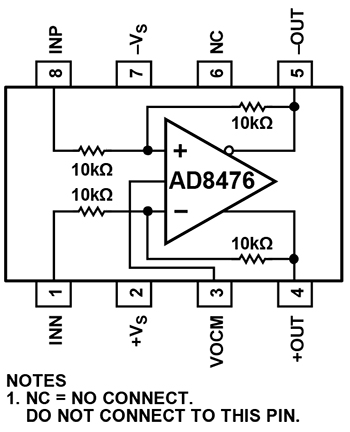
Figure 4: Advanced techniques in 24-bit ΣΔ ADCs, such as the TI ADS124x, have eliminated many of the traditional concerns over use of ΣΔ ADCs in low-latency designs and use with multiplexed differential inputs.
Beyond matching ADC specifications to application requirements, designers can further optimize analog signal chains by considering the role of the voltage reference in applications. By providing a stable reference voltage, precision voltage references are critical for ensuring absolute accuracy in signal conversion. These devices are considered particularly important in applications such as battery-powered designs or energy harvesting designs where supply voltage can fluctuate as the battery reaches the end of its discharge cycle or sources of harvested energy periodically grow weaker.
For applications that do not require this level of absolute precision, designers can eliminate the need for a precision voltage reference by using ratiometric conversion methods (Figure 5). Ratiometric conversion provides a result that is a ratio of the reference voltage – typically the supply or excitation voltage. With this approach, ADC output maintains the ratiometric output even as the supply fluctuates.
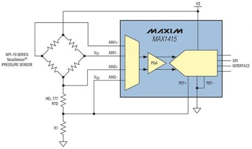
Figure 5: ADCs such as the Maxim Integrated MAX1415 can operate in ratiometric mode, eliminating the need for a precision voltage reference for signal conversion.
Digital Domain
ADCs typically provide a standard I²C- or SPI-compatible serial interface for connecting the output of the analog signal chain to an MCU. As data points stream into the MCU, designers can sharpen the signal-to-noise ratio using conventional filtering algorithms running in software or on digital-signal-processing hardware for more performance-intensive applications.
The ability to create very sharp cutoff and notch filters digitally also provides a significant opportunity to relax requirements in the analog signal chain. For example, designers can elect to shift filter complexity to the digital domain rather than increase the design’s footprint with more complex analog filtering components that might be required in a particular application. Of course, increased software complexity carries burdens of its own in terms of memory requirements and MCU performance capabilities.
Conclusion
Designers can find analog signal conditioning and conversion components with performance specifications that can address the most demanding requirements for data acquisition. For many applications, however, the signal chain can be effective in meeting application requirements without requiring a full complement of components all featuring the best possible specifications. By matching ADCs to conversion requirements and signal conditioning components to ADC specifications, engineers can design signal chains able to easily meet both performance and cost targets.