


The basic laws of thermodynamics ensure that no electronic device can achieve 100% efficiency- although switch-mode power supplies come close (approaching 98%). Unfortunately, anything that generates RF power cannot presently boast such near-ideal performance as there are simply too many impediments to converting DC power into RF power, from losses incurred throughout the signal path, to operating frequency, the inherent characteristics of the device.
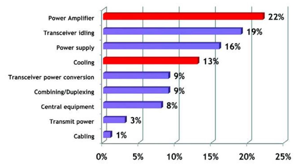
Not surprisingly, every manufacturer of RF power products, from semiconductors to amplifiers to transmitters, along with universities and the Department of Defense, spends enormous amounts of time and money every year to increase the efficiency of RF power generation. And for good reason: Even small increases in efficiency increase operating time in battery-powered products and reduce the annual electricity bills of wireless base stations. Figure 1 shows just how much the RF portion of a base station contributes to power consumption.


Fortunately, these efforts are delivering results that continue to increase RF efficiency every year, some at the device level and others through use of techniques such as envelope tracking, digital pre-distortion/crest factor reduction schemes, and higher classes of amplifiers beyond the ubiquitous Class AB.
A major change in amplifier design, which has in 5 years become the standard in base station amplifiers, is the Doherty architecture. Essentially dormant, it has been used in only a few applications since it was invented by W.H. Doherty of Bell Labs in 1936. Doherty’s research produced an amplifier architecture that delivers very high power-added efficiency with input signals that have high peak-to-average ratios (PARs). In fact, when properly designed, a Doherty amplifier can produce increases in efficiency of 11% to 14% when compared to standard parallel Class AB amplifiers.
Of course, in 1936 and for many succeeding years, only a few signal types possessed these characteristics, as the modulation schemes employed in communication systems were AM and FM. Today virtually every wireless system produces high-PAR signals, from WCDMA to CDMA2000 and any system employing Orthogonal Frequency Division Multiplexing (OFDM), such as WiMAX, LTE, and the latest flavors of Wi-Fi.
A classic Doherty amplifier (Figure 2), which falls into the class of load modulation architectures, actually consists of two amplifiers: a carrier amplifier biased to operate in Class AB mode, and a peaking amplifier biased to operate in Class C mode. A power divider splits the input signal equally to each amplifier with a 90-deg. difference in phase. After amplification, the signals are rejoined with a power combiner. Both amplifiers operate during the peaks of the input signal and are each presented with a load impedance that enables maximum power output.
However, as the input signal decreases in power, the Class C peaking amplifier turns off and only the Class AB carrier operates. At these lower power levels, the Class AB carrier amplifier is presented with a modulated load impedance that enables higher efficiency and gain. Major advances in Doherty amplifier design have been made in rapid succession as the architecture has been rejuvenated, which has led to its unbridled success.
Of course, no architecture is perfect and the linearity and output power are both somewhat less in a Doherty amplifier than in a dual Class AB amplifier. Which brings us to another important circuit that has also become essential for today’s communications environment: analog and digital linearization techniques, the most widely used being digital predistortion (DPD), sometimes in combination with crest factor reduction (CFR). Both DPD and CFR dramatically reduce the Doherty’s distortion, and careful device and amplifier design can minimize the reduction in linearity. However, their use is not strictly defined to use in Doherty amplifiers, as benefits are apparent in other amplifier architectures as well.
Getting It Straight
Modern digital modulation techniques demand high amplifier linearity, without which intermodulation distortion occurs that degrades signal quality. Unfortunately, amplifiers perform best when they are driven near their saturation level, after which they become nonlinear, RF power output decreases with increases in input power, and significant distortion begins to appear. This distortion causes interference to adjacent channels or services. As a result, designers typically back-off RF output power into a “safe zone” to ensure linearity. When they do that, more RF transistors are required to deliver a given RF output power, which in turn increases current consumption and results in less battery life or in a base station, higher operating costs.
DPD effectively introduces “inverse distortion” into the amplifier’s input, cancelling the amplifier’s nonlinearities. The result is that the amplifier need not be backed-off from its optimum operating point, potentially negating the need for more RF power devices. As the amplifier is more efficient, benefits are obtained in both reduction of cooling overhead and in the all-important power consumption. CFR also functions to keep a check on distortion by reducing the peak-to-average ratio of the input signals, reducing signal peaks so that the signal can pass through the amplifier without clipping or distortion. When DPD and CFR are used together, even greater benefits can be achieved.
The Outphasing Approach
Another technique, once again developed and patented nearly 80 years ago by Henri Chireix and typically referred to as “outphasing” (a member of the load modulation family of techniques), is being used by Fujitsu, NXP, and others to increase amplifier efficiency. It combines two nonlinear RF power amplifiers with the two amplifiers driven by signals of different phases. The phases are controlled so that when the outputs are combined, benefits in efficiency can be achieved when using Class B RF power amplifiers. Prudent design techniques, especially proper selection of reactance, allow such a system to be optimized to a specific output amplitude, which can result in improvements in efficiency by a factor of two (theoretically at least).
Fujitsu announced last year that it has applied outphasing in a power amplifier, integrating a compact, low-loss, power-combining circuit with a DSP-based phase error correction compensation circuit that enables transmission across more than 95% of transmission duration in comparison with the 65% typically achieved by existing amplifiers. The design was tested and achieved a power amplifier with a peak output of 100 W; average electrical efficiency was increased from 50% to 70%.
The input signal is split into two signals with constant amplitude and phase variation. Amplitude is set for the RF power device and the power-combining circuit reconstitutes the waveform of the source signal. Previously, combining losses of the precision required to establish the phase difference, when the source signal is reconstituted, had prevented the technique being used commercially. The combiner used by Fujitsu has a shorter signal path that reduces loss and increases bandwidth.
Promising Developments at NXP
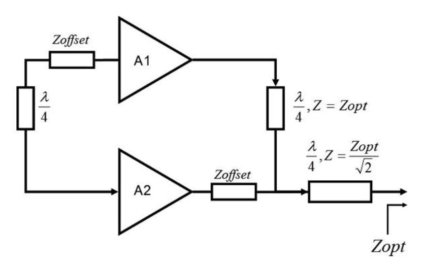
Another variation on the outphasing theme that has no load modulation effect is called a Linear Amplification Using Nonlinear Concepts (LINC), employs an isolating combiner and amplifier stage driven to saturation, and is effective in increasing linearity and peak efficiency. LINC amplifiers suffer from relatively low efficiency because each amplifier operates at a constant power, even at low RF output levels. This is what Chireix fixed by combining outphasing with a non-isolating combiner and load modulation, thus increasing the average efficiency. NXP Semiconductors has taken this a step further by using outphasing to control two switch-mode RF amplifiers so that they accommodate signals with high crest factors. The company is combining the Chireixoutphasing technique with GaN HEMT switch-mode Class E amplifiers (Figure 3).
NXP developed and patented a new driver technology to control the phase relationship that allows the amplifier to achieve high efficiency over a bandwidth of about 25%. This results in an architecture that combines Class E amplifiers and load modulation to maintain high efficiency when the amplifiers are backed off from saturation, which makes them able to accommodate a variety of complex waveforms. NXP offers reference designs for Class E RF power amplifiers based on GaN devices along with information about the Chireix technique.
Envelope Tracking
Still another arrow in the quiver of amplifier designers is envelope tracking, in which the voltage applied to the power amplifier is continuously adjusted to make sure that it is operating in its peak operating region and thus at maximum power. In contrast to a typical power amplifier design in which a DC-to-DC converter supplies a fixed voltage, an envelope tracking power supply modulates the power supply connection to the amplifier with a high bandwidth, low-noise waveform that is synchronized to the instantaneous envelope of the signal.
There is considerable interest in applying envelope tracking to CMOS RF power devices. Nujira has been developing this technology for many years. They have demonstrated that the technique can overcome the negative characteristics that have impeded the use of CMOS for RF amplifier applications with respect to linearity. CMOS power amplifiers have been a poor choice for modern highPAR modulation techniques because they have inherently poor linearity, which requires them to be backed off to reduce distortion. And when CMOS amplifiers operate at higher RF power levels, distortion clips the peaks of the waveforms.
However, Nujira has combined its proprietary envelope-tracking technology with its patented ISOGAIN linearization technique to eliminate the linearity problem without the use of DPD. Devices using this technique have achieved high efficiency with equal performance in other areas to that of GaAs. The benefit of all this research into CMOS is that CMOS is ubiquitous throughout the electronics industry, supported by many foundries, and is thus comparatively inexpensive. Since it is based in silicon, it can also incorporate control and bias circuits directly on the die of the power amplifier.
And Now for Something Entirely Different
Yet another amplifier technology is being championed by Eta Devices, which was spun off from Massachusetts Institute of Technology and cofounded by two MIT Electrical Engineering professors, Joel Dawson and David Perreault, and a former power amplifier researcher from Ericsson and Huawei. Its Asymmetric Multilevel Outphasing (AMO) technology was developed at MIT and the company is funded by Ray Stata, cofounder of Analog Devices and his venture firm, Stata Venture Partners.
Eta Devices makes bold claims for its technology, called ETAdvanced (Envelope Tracking Advanced), projecting that it could reduce base station energy costs by 50%. Another claim is that it can double the battery life of smartphones. The premise is that the RF power transistors in amplifiers consume power in both standby mode and when transmitting, and that the only way to improve their efficiency is to reduce standby power to its lowest possible level.
The act of moving between low-power standby to high-power output creates distortion that current systems keep in check by maintaining high standby power levels, at the cost of high power consumption. The Eta Devices approach, however, chooses different voltages across the transistor by sampling them up to 20 million times per second, and selecting the one that minimizes power consumption.
Another issue that the company addresses is that LTE Advanced and its 100 MHz bandwidth requirement will place enormous demands on RF power amplifiers. Envelope tracking alone cannot accommodate this, as it cannot support channels broader than 40 MHz.ETAdvanced supports channels of up to 160 MHz wide, so it can serve both LTE Advanced and 802.11ac Wi-Fi, according to the company. A base station using its technology is very small and the company claims that it has developed the first LTE transmitter with average efficiency greater than 70%.
Summary
Work being conducted into increasing the efficiency of RF power generation, if described completely, could fill a large book. Efforts are underway not only in the areas discussed in this article, but in the use of different classes of amplifiers and assorted techniques that are combined to produce interesting results. Regardless of how these advances are achieved, one certainty is that the search for higher and higher efficiency will continue for as long as there is demand for ever higher data rates.