


Apparent, Reactive, and Active Power
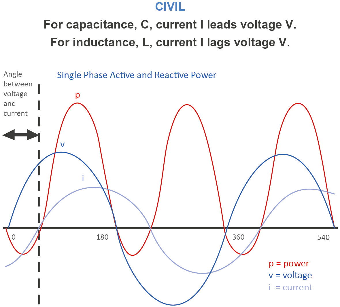
Electrical power can be measured in Watts by multiplying voltage times current, but it is an accurate calculation of usable power only in purely resistive circuits. When input current and voltage waveforms are misaligned or out of phase due to the reactance of an energy storage element (i.e., an inductive or capacitive load), then this simplistic relationship no longer holds true.


The effect of misaligned voltage and current waveforms is that the full amount of applied power (apparent power) cannot be delivered to the load as useable or active power, because some of the energy is recirculated or reflected back into the supply (reactive power).
The figure below demonstrates this graphically and provides a nice mnemonic (CIVIL) for remembering the current/voltage lead or lag relationship based on the type of reactive element.
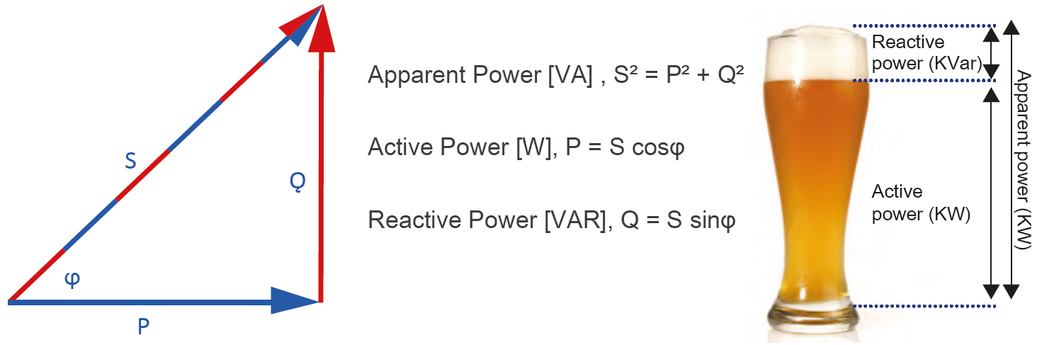
These concepts and their relationship are highlighted in the figure below both mathematically and graphically, in terms of a beer glass (the head on a beer does no “work”).
What is Power Factor Correction (PFC)?
Power factor (PF) is defined as the ratio of active power to apparent power (or cosine of the phase angle between the waveforms shown as ϕ in the figure above). Think of it as the percentage of available power that actually makes it to the load, which raises the following question: What happens to the rest of the power (1 – PF)? Physics tells us if this “other” power is not going to the load, then it must go elsewhere, i.e., it is reflected back into the supply and not used. An ideal PF (1) can only be achieved when there is a phase angle of 0° between the voltage and current waveforms, meaning all the supplied energy is used by the load and none of it is reflected back into the supply.
These concepts and their relationship are highlighted in the figure below both mathematically and graphically, in terms of a beer glass (the head on a beer does no “work”).
So, if the power factor is as close to one as possible, we maximize the usage of the supplied power. Power factor correction (PFC) is the term given to circuits that realign the current and voltage waveforms to improve the power factor. PFC solutions can be either passive (e.g., adding inductance to counteract the effect of a mainly capacitive load) or active (using switching transistors to control the current waveforms).
Something to note is the motivation for PFC. Most electricity meters only measure the active power consumed and ignore the reactive power; however, the electricity utility provider must still supply enough headroom to cover the instantaneous power consumption, including the reactive elements. Therefore, minimum PF requirements are typically dictated by edict (e.g., rules and regulations) due to the pressure from utility providers to cut their electricity generation and transmission costs. Otherwise, no manufacturer would opt to add cost (or even take a small, overall efficiency hit) to their power supply. In fact, PFC solutions will mostly go against the cardinal value propositions of maximizing the size, weight, and power (a.k.a. – SWaP) factors, since a PFC front end takes up space and adds to the overall losses. So, in short, most engineers add it because they must, not because they want to!
PF Contribution to Harmonics & THD
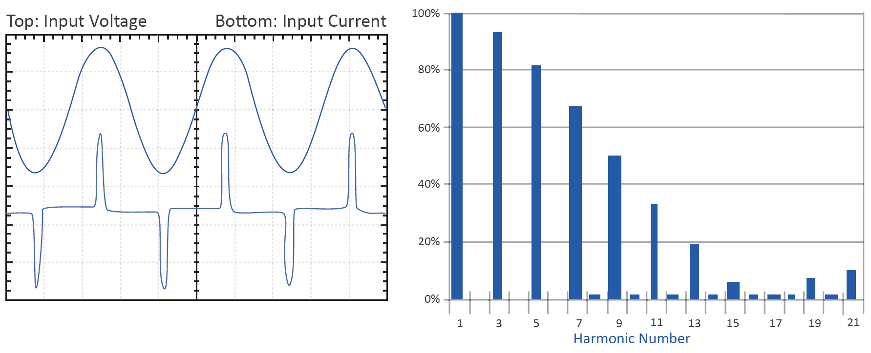
We will now get back to the question about where all the reactive power goes. The input voltage and current root-mean-square (RMS) waveforms are sinusoidal waveforms that can be represented as being comprised of an infinite series of periodic functions at harmonic frequencies of the fundamental (these harmonics are called the Fourier Series [2]). Even-numbered harmonics cancel out, so all this harmonic energy is seen at odd-numbered harmonics only. The majority will typically be seen at the third harmonic (i.e., first odd harmonic after the fundamental) and it tends to decrease as you go up in the series. These harmonics cause distortion to the input voltage and current waveforms, the sum of which is known as total harmonic distortion (THD). A lower PF implies greater distortion on the input line, which is why use cases that may install many power supplies on the same input circuit have higher PF minimum rating requirements. NOTE: Power solutions meeting all proper regulatory limits can still be a liability to power line quality when scaled to too many units in volume. Even with very high PF (i.e., >0.98), the cumulative effects of the reactive components will eventually become significant in high enough volumes.
How far out in frequency to look will depend on your fundamental frequency, but it may easily extend into radio frequencies (RF). Since this RF energy is emitted as conducted (back onto the line) and radiated (into space) electromagnetic energy, there are international standards/regulations governing compliance with electromagnetic energy emissions limitations at specific frequencies. The table below summarizes some of these references and where they can be found. The majority focuses on electromagnetic compatibility/compliance (EMC) limits for electromagnetic interference (EMI), so one can look at the various frequency ranges and limits to understand what they are up against.
While a bit tangential, it should also be noted that the impact of RF emissions goes both ways. While most attention is put into ensuring EMC for the system or device under test (DUT), the DUT can also be susceptible to external RF from the environment. An example of such susceptibility is the bombardment of high-energy radiation particles (typically from space), which drives designers to build immunity (e.g., radiation-hardened or “rad-hard”, in this example) into their designs and perform susceptibility testing as part of the qualification process.
Quick Overview of PFC Solutions
If you recall from our CIVIL mnemonic, capacitance causes the current waveform to lead the voltage waveform and vice versa for inductance, which means that we can use these elements to shift the phase angle in one direction or the other in pursuit of maximum PF. Directly using these energy storage elements on the input of a power supply is known as passive PFC. Using elements with a semiconductor switch (essentially adding an extra switching power supply at the input) is known as active PFC.
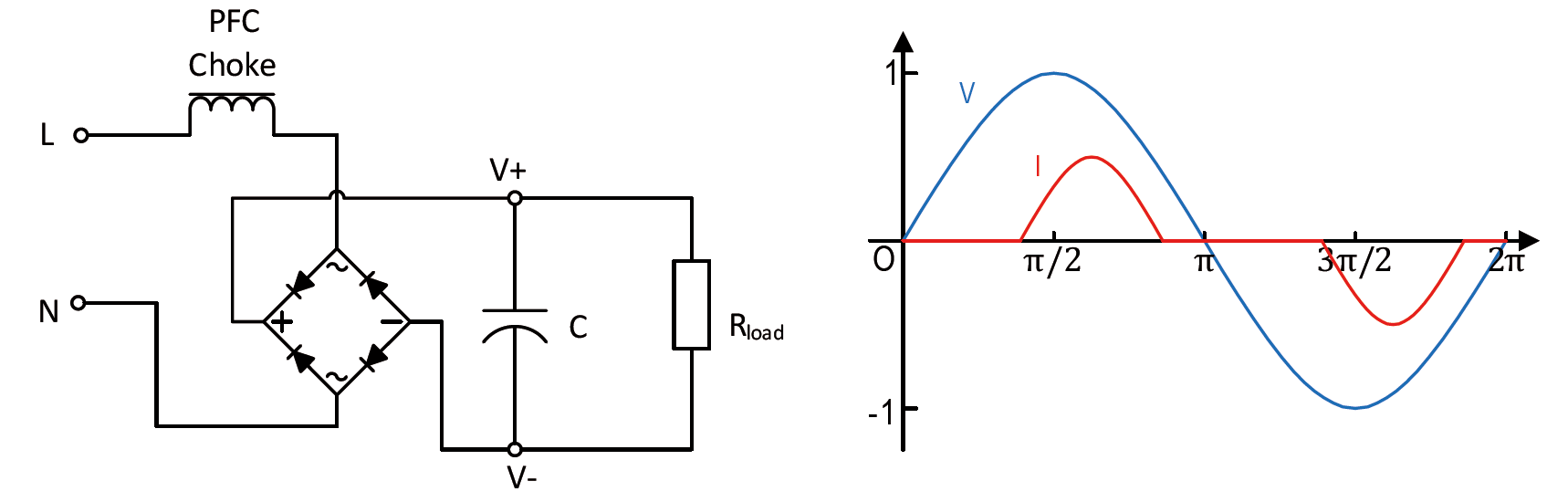
The simplest form of passive PFC is adding a series inductor (a.k.a. – PFC choke) before the rectification stage of the power supply as shown in the figure below with the resulting waveform. While this is simple, its disadvantages include typically requiring a larger/heavier inductor, along with limiting the max achievable PF to ~0.7 (versus ~0.4 without any PFC). Additionally, the PFC choke must be sized for a limited input voltage range, which is undesirable for supporting universal ac-input scenarios and again, driving a larger/heaver solution.
Active PFC solutions mitigate most of the disadvantages just mentioned. The most common topology for active PFC is the boost (a.k.a. – step-up) converter. Within this class of power conversion are a handful of topologies (i.e., discontinuous conduction mode or DCM, continuous conduction mode or CCM, and critical conduction mode or CrCM or boundary mode) for implementing active PFC, but a comprehensive overview of these is beyond the scope of this discussion and can be found in [1].
A boost converter will increase the voltage on the input capacitor and keep it charged across a wide range of input voltages, thus supporting universal ac compatibility. It will try to achieve unity PF by ensuring that the average input current through the PFC choke closely follows the input voltage via one of the topologies referenced above. Each topology has its own tradeoffs regarding SWaP factors and EMI impact. The figure below shows an example of an active PFC circuit driven by a dedicated controller with input and output voltage waveforms.

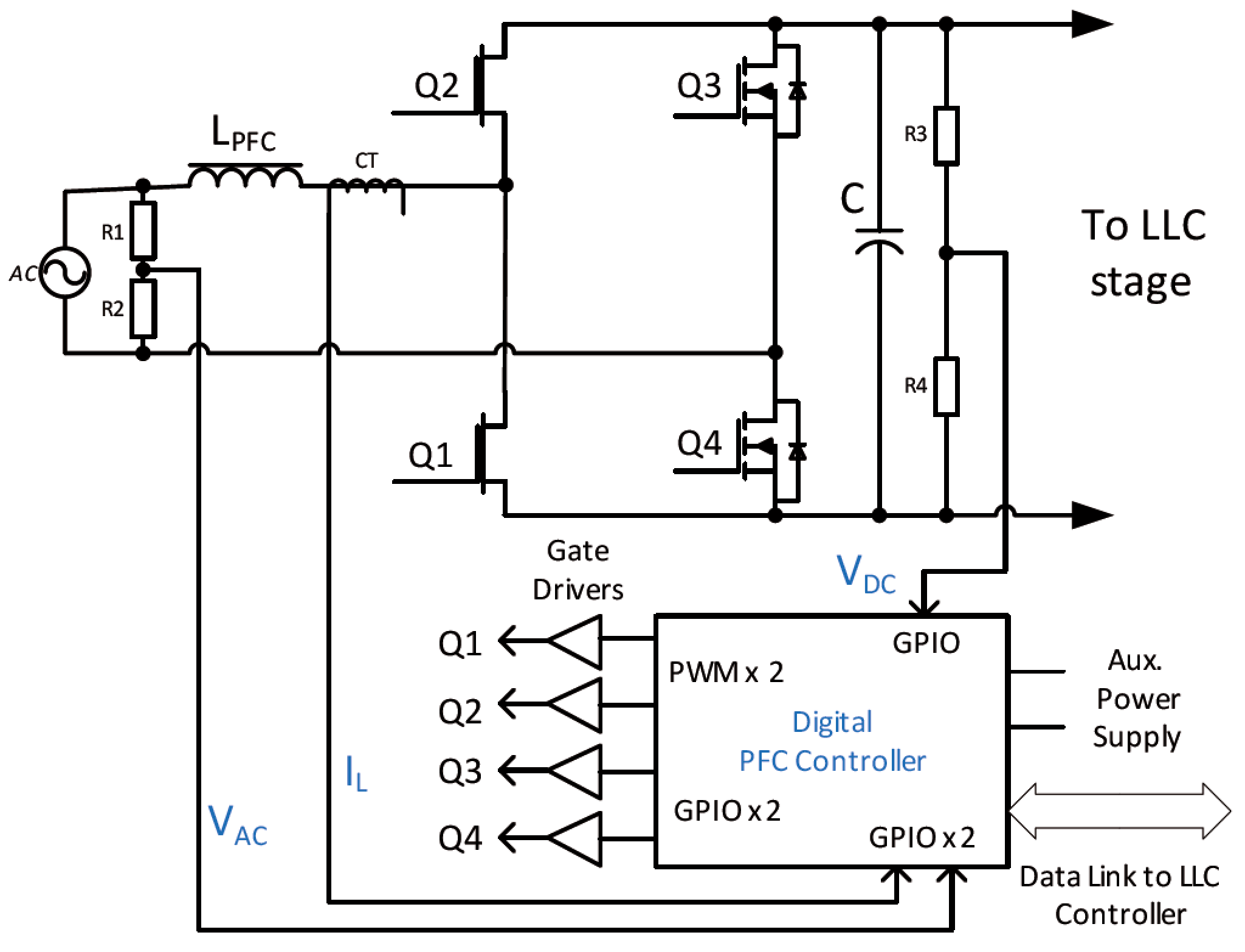
A more modern take on the active PFC takes advantage of a unique property of gallium nitride (GaN) switches, which lack a body diode (unlike silicon MOSFETs) used to form a rectifier bridge and thus enable a higher-efficiency PFC implementation. This is known as a bridgeless PFC (a.k.a. totem-pole PFC), and an example circuit with its controller block is shown in the figure below, showing the difference between the GaN and Si switches.
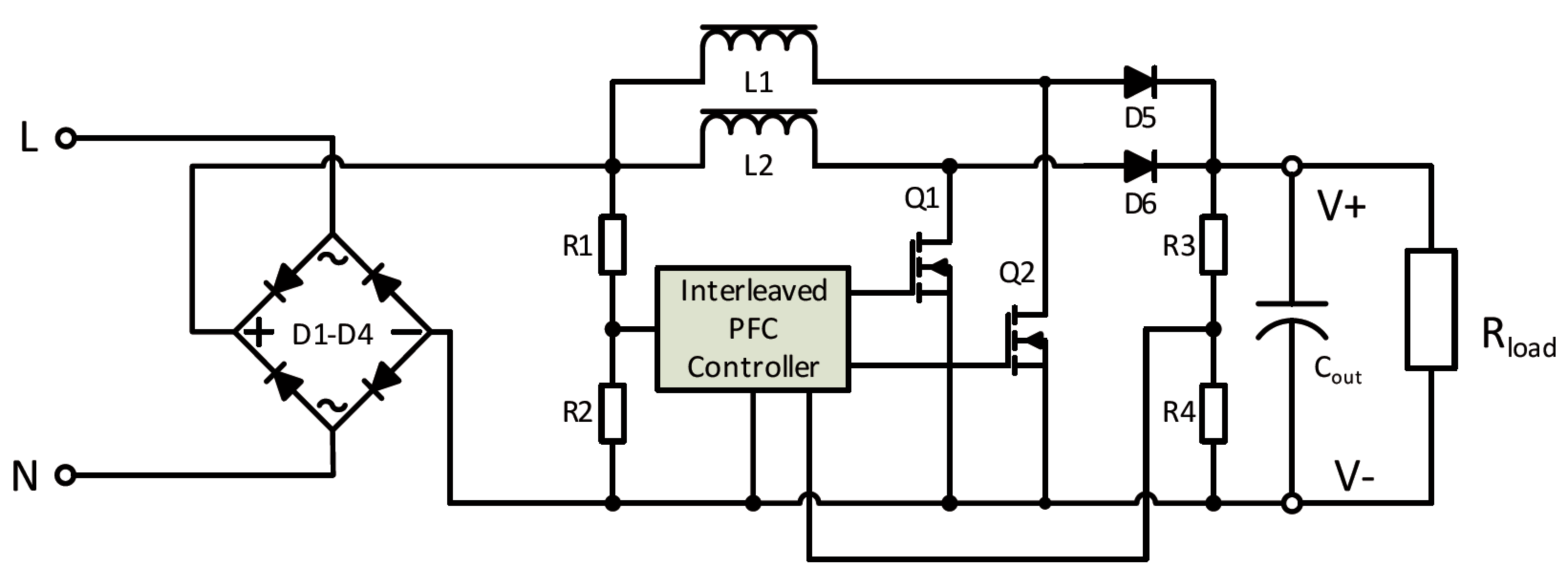
A final consideration for PFC implementations is to take advantage of the benefits offered by multiphase power converters, such as reduced thermals and component stresses, by halving the current processed by each leg and combined at the output out of phase with each other. A larger PFC (typically characterized/dominated by the magnetics) can be sized for half the full-rated current and interleaved in two equal phases.
Whether one is trying to maximize their EMC performance and/or ensure acceptable line quality on distributions with high numbers of units on a single input bus, PFC is more than a “nice-to-have” feature and should be given serious consideration as part of an overall power solution and deployment.
Courtesy: RECOM