


Description
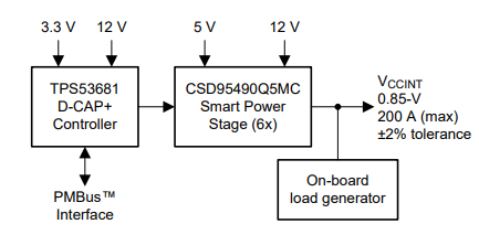
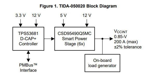
This reference design uses the TPS53681 multiphase controller and CSD95490Q5MC smart power stages to implement a high-performance design to power the 0.85-V, 200-A, VCCINT rail of a Xilinx Viretex Ultrascale+ FPGA. The secondary output of the controller can be used to power an auxilliary rail of the FPGA. The smart power stages and integrated PMBus allow for easy output voltage setting and telemetry of key design parameters. The design enables configuration, VID adjustment, and compensation adjustment of the power supply, while providing monitoring of input and output voltage, current, power, and temperature. TI’s Fusion Digital Power Designer is used for programming, monitoring, validation, and characterization of the system.


 Features
- Six-phase design targets high-power main FPGA core rail
- D-CAP+ modulator for superior current-sharing capabilities and transient response
- PMBus compatibility for output voltage setting and telemetry for VIN, VOUT, IOUT , and temperature
- Dual rail temperature monitoring for independent tracking of thermal performance
- Full compensation tuning through PMBus
- Peak efficiency of 92% for VCCINT rail at VOUT =0.85-V ( nom )
Applications
- Hardware Accelerator Cards
- Data Center Switches
- Campus and Branch Switches
1 System Description
This is a power-dense, high-performance design targeted at powering Xilinx Ultrascale+ FPGAs commonly found in demanding datacenter switches and hardware accelerator card applications. These processors require excellent thermal performance, efficiency, and a fast transient response from their voltage regulators while also requiring on-the-fly optimization through PMBus. This design meets all the criteria with a simple thermal solution and minimal number of output capacitors despite an extremely tight regulation window thanks to the performance of TI’s D-CAP+ modulator. The dual-output multiphase controller and TI’s proprietary smart power stages allow for an integrated design, which, when compared to more traditional discrete designs, eliminates a number of passive components and reduces the printed circuit board (PCB) layout area.
1.1 Specifications and Block Diagram
1.3 Highlighted Products
1.3.1 TPS53681 – Dual-Channel (6-Phase + 2-Phase) or (5-Phase + 3-Phase) D-CAP+ Step-Down Multiphase Controller with NVM and PMBus
- Easily configurable for a wide range of dual-output voltage scenarios
- Programmable loop compensation through PMBus
- Configurable with non-volatile memory (NVM) for low external component counts
- Dynamic phase shedding with programmable current threshold for optimizing efficiency at light and heavy loads
- PMBus system interface for telemetry of voltage, current, power, temperature, and fault conditions
- Dual-rail temperature monitoring
- 5-mm × 5-mm, 40-pin, QFN PowerPad package
1.3.2 CSD95490Q5MC – 75-A Synchronous Buck NexFET Power Stage With DualCool Packaging
- 75-A continuous current capability
- 95% system efficiency at 25 A
- Up to 1.25-MHz switching frequencies supported
- Temperature-compensated bidirectional current sense signal
- Analog temperature output and fault monitoring
- High-density, low-inductance, SON 5-mm × 6-mm package
1.3 System Design Theory
The D-CAP+ modulator of the TPS53681 controller is integral to the high-performance of this reference design. This modulator allows the control loop to remain stable over a wide range of operating conditions as its transfer function is insensitive to variations in input voltage, load current, and phase number. A phase margin of 81.6° was measured for the VCCINT rail with a crossover frequency of 99.5 kHz. Placing the unity gain frequency higher than 1/10 the switching frequency allows for a faster transient response. This faster transient response allows VOUT to remain within its regulation limits during large load steps, such as the 100-A step specified by Xilinx. The output maintains stability even as the load current duty cycle and frequency vary. A faster transient response directly reduces the number of output capacitors required as compared to older regulation topologies such as peak current mode and voltage mode control.
Loop compensation can be adjusted easily using the PMBus interface through TI’s Fusion Graphical User Interface (GUI). The GUI allows the user to tune the design for a wide range of output filters, including using all ceramic output capacitors, in case the design requirements change. At high load currents, the DCAP+ modulator can maintain an even balance of all phase currents to avoid thermally stressing or damaging either the field-effect transistors (FETs), inductors, or FPGA while maintaining tight output voltage regulation.
The CSD95490Q5MC smart power stage features an optimized driver-FET solution in a thermally-efficient package which provides high efficiency up to 75 A of DC load current. The design process for the thermal solution becomes much simpler than using less efficient power stages or discrete FETs. The lower switching and conduction losses lead to higher efficiency and thus excellent thermal performance. The excellent thermal performance allows for smaller heat sink requirements and less airflow to be implemented in the final system design. Integrated temperature and fault monitoring from the power stage to the TPS53681 controller allows for operational telemetry, debug, validation, and configuration of the design through PMBus. On-chip, temperature compensated, bidirectional current sensing offers increased accuracy over operational corners compared to older, potentially uncompensated, DCR sense methods.
The regulator layout and output capacitor selection for this design received special consideration. Common bulk capacitors with 6 mΩ or 9 mΩ ESR values do not meet the tight regulation tolerances for this design during transient events. Instead 3-mΩ capacitors ensure a low-output impedance and specification compliance while maintaining a resonable component count.
These bulk capacitors, along with additional ceramic capacitors, are placed as close as possible (within 2 to 3 inches) to the load to maintain minimal board impedance and optimal performance. This layout also includes wide output and ground planes on multiple PCB layers to help minimize board parasitics. With no DC load line and a ±2% tolerance on VOUT every millivolt matters. Proper layout and component selection becomes even more of a priority for these types of high-performance designs.
1 Hardware, Software, and Test Results
1.1 Required Hardware and Software
1.1.1 Hardware
The hardware requirements for this design are the same as those listed in the TPS53681 EVM User Guide on page 12.
1.1.2 Software
This design uses TI’s Digital Fusion Power Designer software.
1.2 Testing and Results
1.2.1 Test Setup
The setup for testing this design follows the guidelines set forth in the TPS53681 EVM User Guide.
1.2.2 Test Results
1.2.2.1 Efficiency and Power Loss
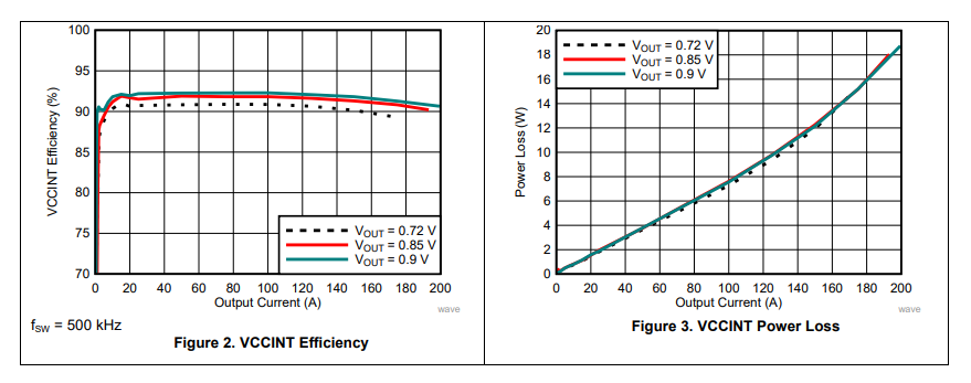 Efficiency and loss curves were measured, with inductor and 5-V loss included, for the nominal, minimim, and maximiu output votlages. Due to dropout limitations with the electronic load, 200-A could not be achieved at output voltages of 0.72 V and 0.85V, so the results show only up to the maximum load that was sustainedat each voltage.
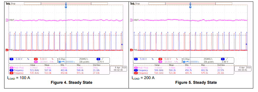
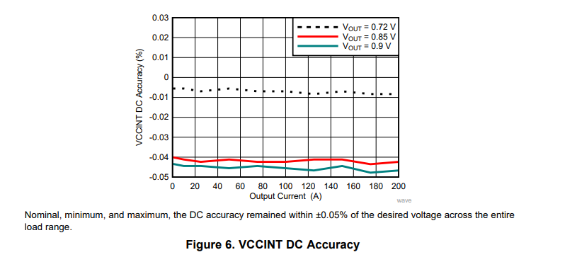
1.2.2.2 Steady-State Regulation and DC Accuracy
The output voltage was tested for steady-state stability across the entire load range without recording any failures or anomalies. DC ripple remained within the design targets and the measured switching frequency was within the data sheet limits.
 1.2.2.3 Switch Node Ringing
Switch node ringing of this design was checked to ensure long term robustness. Ringing above or below the CSD95490Q5MC datasheet limits could damage the power MOSFETs inside the power stage over time. Eventually, performance would decline and complete failure is possible.
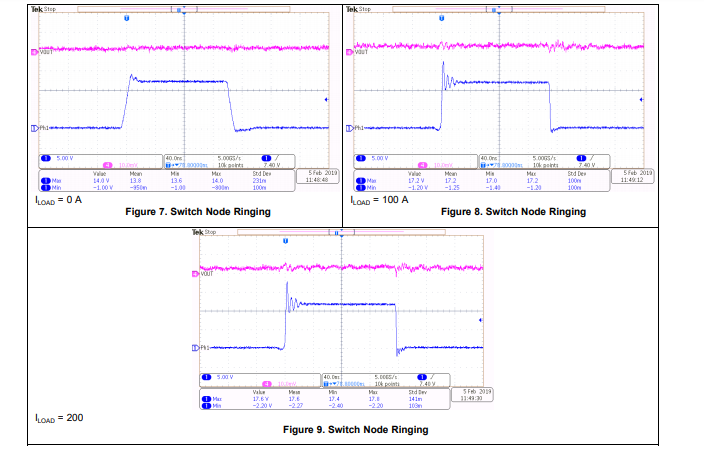
Over the full load range, the ringing on the rising and falling edge of the switch nodes was observed to be within the Absolute Maximum Ratings of the power stage datasheet without the use of a boot resistor or snubber on each phase. Only a small 0402 sized 4700 pF input decoupling capacitor was placed close to the VIN pins of each power stage to help reduce ringing. However, switch node ringing is highly dependent on PCB layout and so placeholders for boot resistors and snubbers are recommended for every design in case differences between the end application board and the board used for these measurements increases ringing.
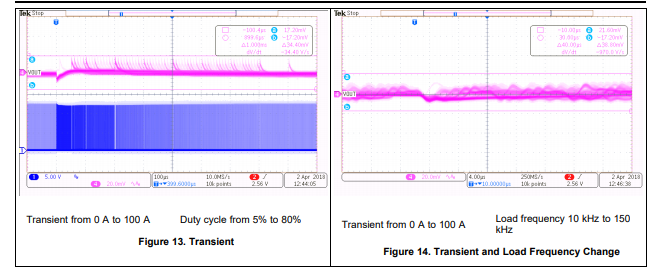
1.1.1.1 Transient Response
A load transient circuit placed on the board close to the output of the VCCINT rail was used to generate the 100-A step at the slew rate of 100A/μs. The single-step response showed little to no undershoot and the overshoot was less than the allowable 17 mV.
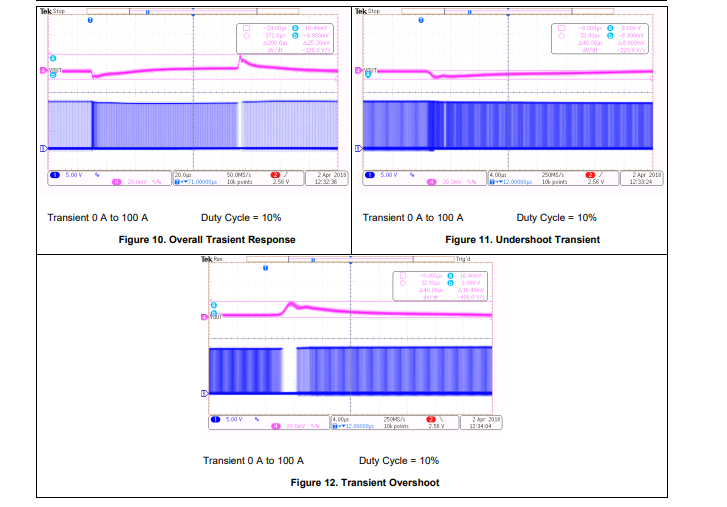 The output voltage remained stable as the load duty cycle sweeps from 5% to 80%. Minimal undershoot was measured and the overshoot was less than 17 mV. While the transient circuit was able to hit the quick slew rate, it could not handle load frequencies above 150 kHz and so a beat frequency check at 500 kHz could not be performed. However, Figure 13 shows no instabilities as the frequency of the load step rises to 150 kHz.
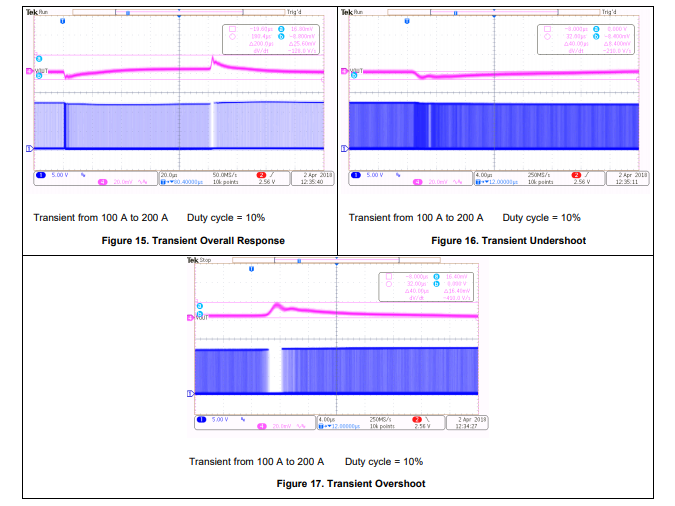
 Identical results occur when aa 100 A to 200 A load step is applied to the regulator output. The peak-topeak excursions, overshoot, and undershoot all remain within the allowable ±2% window.
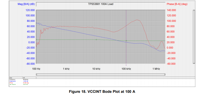
 1.1.1.2 Additional Small Signal Stability Testing
Because high frequency transients can not be generated for this design, a network analyzer is used generate a Bode plot of the loop transfer function and confirm the stability of the regulator. Figure 18 shows a unity gain frequency of 99.5 kHz with a phase margin of 81.6°, indicating good stability with plenty of margin.
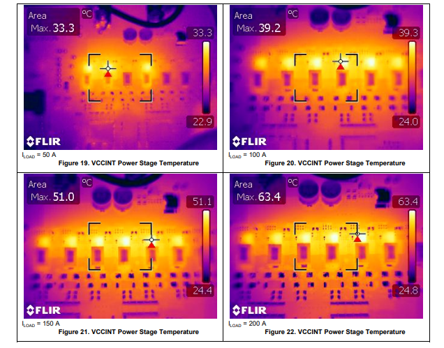
 1.1.1.3 Thermal Performance
The thermal performance of the VCCINT rail is tested for 50 A, 100 A, 150 A, and 200 A loads at the nominal output voltage. The ambient temperature is 22°C for each test case and the design was allowed to soak for 5 minutes under load to reach thermal equilibrium. Airflow across the boards is 200 LFM.
 1.1.1.4 Output Voltage Probing Techniques
Due to the tight output voltage tolerances associated with this application, standard passive and differential probes do not suffice when validating the design. Instead, solder a cut down coaxial cable from the oscilloscope BNC input directly across either an output capacitor near the feedback line sense point, or the feedback lines. (see Figure 23). This procedure yields a much clearer of the output voltage on the oscilloscope when measuring DC ripple and confirming transient response.
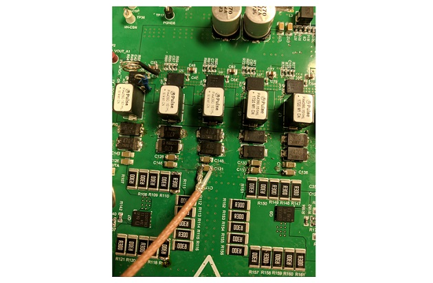 Figure 23. Proper BNC Cable Placement on VOUT
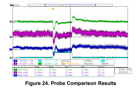
To show the impact that probe type can make, Figure 24 shows a direct connection with a BNC cable compared with passive and differential probes as a load transient is applied to the design.
Using a passive probe (blue trace) slows down the response when compared to the BNC probe by misrepresenting the overshoot upon load release. At the same time, the ringback after the load step is over exaggerated and there is more noise during the steady state portion of the waveform. With this waveform, a designer might incorrectly assume compensation is an issue and make changes that could hurt loop stablity while also undersizing the value of output capacitance (COUT).
Probing the output voltage (VOUT) with a differential probe instead (magenta trace) shows significantly more noise than the BNC probe which falsely reports a peak-to-peak excursion that is 6.4 mV higher than the true value. Using this probing technique, significantly more output capacitance would be needed to keep VOUT within the speficiation range, if it is even possbile. The noise injection from the differential probe might simply be too high, making a passing result unobtainable given the tight tolerances required.
Figure 24. Probe Comparison Results
Article Courtesy: Texas Instruments