


Recent advancements in high-speed Data Converter sampling rates and bandwidth handling capabilities changed the way of interfacing the high-speed ADCs and DACs with processors and FPGAs. The interface between the Data Converters and FPGA/Processors is moved from LVDS to JESD204B high-speed serial interface.

The technological advancements in data converters also provided with a lot of system design advantages. The Giga sampling rate data converters are also called as RF sampling data converters as these data converters can directly handle RF frequencies enabling new possibilities in system architecture for Defence, Test & Measurement, and Communications market.


What are the benefits of RF sampling high-speed ADCs and DACs?
Texas Instruments recently released ADC32RF45 ADC which can support RF input frequencies up to 4GHz and supports sampling rate up to 3GSPS which can be used to directly digitize the L-band/S-band signals for defense radar systems. Similarly, DAC38RF8x DAC can generate the RF outputs up to and beyond 4GHz output frequency. These ADCs and DACs can provide the true software defined radio capability with flexibility for frequency input and output selection, dynamically re-configure different frequencies and multi-band processing. Direct RF Sampling provides lots of flexibility through digital signal processing. These will enable system designers to re-use the same hardware for multiple platforms which reduces R&D costs.
For wideband digital receivers/ transmitters, Test and measurement, Aerospace and defense, 5G mobile communication systems, 802.11ad Wi-Fi systems, higher bandwidth handling capability is a key feature to have and it can be enabled using the RF-sampling ADCs and DACs. The example options for these systems are ADC12J4000 which delivers an instantaneous 2.0GHz bandwidth, ADC32RF45 which delivers 1.5GHz instantaneous per channel bandwidth and DAC38RF8x which can provide more than 4GHz bandwidth.
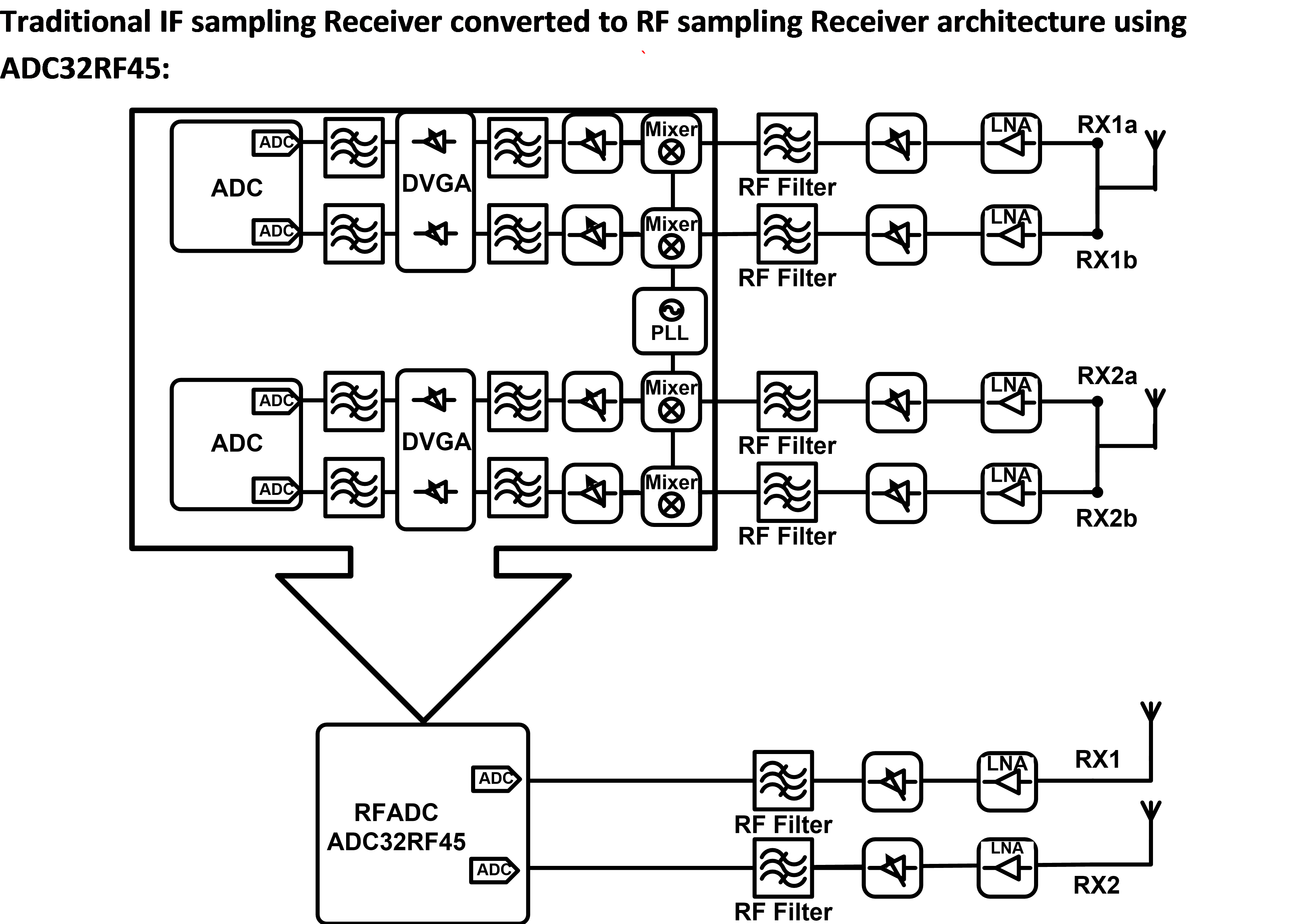
For the receiver applications, ADC32RF45 RF sampling ADC can eliminate up to four intermediate frequency (IF) down-conversion stages in multi-band receivers, reduces board space up to 75 percent and allows to simultaneously processing multiple frequency bands. The below figure provides the top-level functional diagram.
Analog Interface needs for RF Sampling data converters:
As the RF-sampling ADCs handling the direct RF input frequencies, the input stage of the ADCs needs to handle very high frequencies. The high-speed Amplifier (ex. LMH5401 or LMH6401) or Balun is typically used in the front end stage of ADC for converting the single-ended input to differential conversion and similarly for DAC output stage for the differential to single ended conversion. There are tradeoffs between using the Balun/transformer Vs Amplifier for this purpose and the designer needs to carefully select between these two options based on the system performance tradeoffs. Baluns are not suited for wide bandwidth and it will have large insertion loss and varies with frequency compared to wideband high-speed amplifiers. Baluns don’t have any power gain as impedance matching and voltage/current gain are dependent whereas amplifiers support power gain as impedance matching and gain are independent. Amplifiers provide buffering whereas Baluns require the previous stage to drive filter and ADC input load. But Amplifier adds noise compared to Balun. The selection between the Balun and Amplifier needs to be done based on the above parameters and system performance tradeoffs for interfacing with the specific ADC and DAC.
Digital Interface needs for RF Sampling data converters:
As these RF-sampling ADCs and DACs have sampling rates of 4GSPS and beyond, traditional LVDS interface will not be possible to connect these data converters with Processors and FPGAs. For examples, ADC32RF45 is a 14 bit 3GSPS dual Channel ADC. LVDS interface cannot directly support 3gsps interface speed. We need to have new interface type which can support these high data rates. The JESD204B serial interface is developed for solving this interface problem. ADC output or DAC input can connect with FPGA or Processors over the JESD204B interface with the speeds up to 12.5Gbps as per present standard and the speeds might be enhanced further in future as the data converter speeds are going to increase further in coming years. Texas Instruments is fully committed to this new interface standard and offers a compelling data converter roadmap with state of the art devices to support it. The application note SLYY057B ( www.ti.com/lit/SLYY057 ) provides the details on what all you need to know while you are transitioning to JESD204B interface.
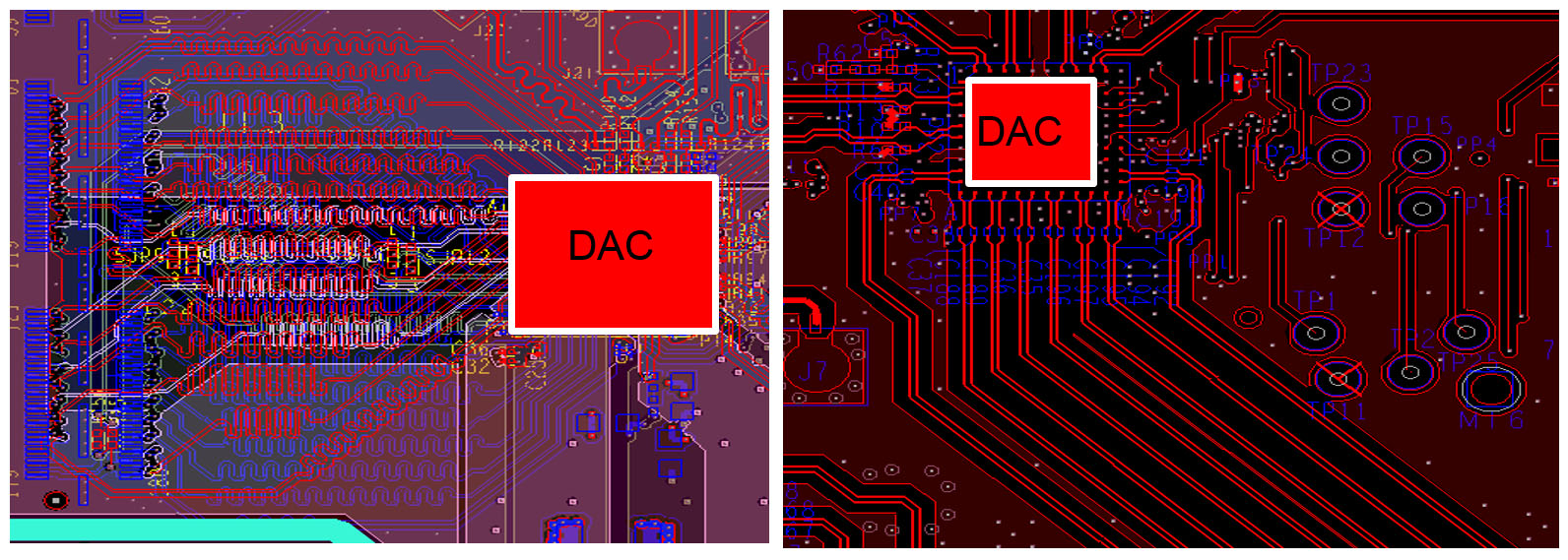
In LVDS and CMOS systems, package size, board area and power consumption dominated by output buffers rather than the data converter itself. JESD204B Interface key benefit over existing LVDS/CMOS interface is reduced IC package pin count for data converters and eventually reduction in PCB layout routing complexity and area. Below layout example clearly shows that the JESD204B (right side) based board has smaller IC package and lesser PCB routing complexity.
JESD204B serial interface has 3 subclasses called Sub class 0, sub class 1 and sub class 2. Sub class 2 uses SYNC as timing signal and due to SYNC timing constraints, it can be used only for data converters sampling rates upto 500MSPS. For RF sampling ADCs and DACs, the sub class1 which uses the SYSREF is required. Deterministic Latency is supported in JESD204B subclass 1 and 2 which is critical for applications like beam forming etc. where multiple data converters are used in the system and synchronization between these multiple data converters is needed. The inherent advantage of JESD204B is that they are no length matching requirements for the data outputs from ADC to processor/FPGA.
The clocking is important device for JESD204B data converters clocking along with clocking FPGA/processor by providing Device clock and SYSREF clock. TI LMK0482x clocking devices are specifically designed for this purpose and widely used in the industry for JESD204B clocking.
How system designers can quick start designs with RF sampling ADCs?
There are multiple TI reference designs using RF sampling ADCs and DACs interfacing with FPGAs/processor. Many technical publications, application notes are also available to understand JESD204B interface and deterministic latency and designing the solutions to achieve deterministic latency. The following are some of the examples of reference designs.
- TIDEP00081: TI Design showing Wideband receiver solution using TI processor 66AK2L06 (multicore processor DSP+ARM) interfacing directly with ADC32RF80 over JESD204B (http://www.ti.com/tool/tidep0081).
- TIDA-00826: TI Design with RF sampling ADC and its analog front end solution using High speed Amplifiers (http://www.ti.com/tool/TIDA-00826).
- TIDA-00432: TI Design showing the synchronization of JESD204B Giga sample ADC with FPGA for Phased array radar systems (http://www.ti.com/tool/TIDA-00432).
The following application notes will be useful for understanding the JESD204B interface, its benefits, deterministic latency and usage for high speed data converters.
- SLYT628 : JESD204B multi-device synchronization: Breaking down the requirements.
- JESD Blog stories: This has very useful JESD204B based blogs for system designers. http://e2e.ti.com/tags/JESD204B%2bseries