As the Applications for 5G Expand Due to Its Increased Performance, the Circuits inside Devices Are Dramatically Growing in Size
Commercial service for the 5th generation mobile communication (5G) has finally started. The performance of smartphones has been greatly enhanced with ultra-high speed, large capacity, ultra-low latency, and multiple simultaneous connections, and new applications are expected to grow, such as rapid downloading of 4K-quality video data, communication using virtual reality (VR), and linkage between computers and machines in remote locations. Moreover, there are high expectations for the use of 5G as an element in the communication infrastructure for realizing a prosperous and low-waste society by encouraging the use of data in factories, medical facilities, and social infrastructure.


5G-enabled smartphones will likely incorporate electronic circuits with more diverse and complex structures than ever before. In terms of cellular communication functions alone, they need to support the Sub-6 band (3.7 GHz and 4.5 GHz), the 28 GHz band (millimeter wave band), and the existing 4G band. In addition, circuits are needed to utilize Bluetooth®, Wi-Fi, and Near Field Communication (NFC) for data communication with peripheral devices, and GPS to detect location. Assuming that 5G smartphones will use these diverse and high-precision wireless communication functions, these smartphones will be equipped with high-performance cameras and displays, as well as sensors and signal processing circuits necessary to utilize new applications such as VR and AR (Figure 1). Consequently, this will dramatically increase the size of the electronic circuitry inside the device.
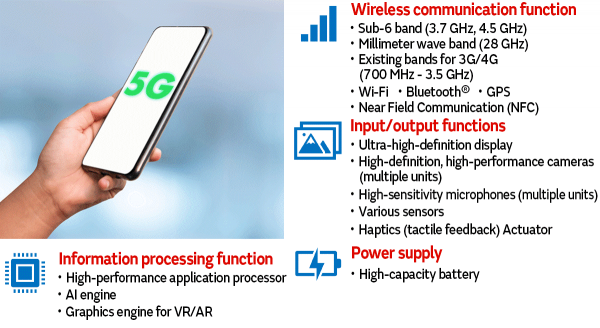 Figure 1. Examples of functions to be incorporated in 5G-enabled smartphones
Miniaturization of the Electronic Components Making up Internal Circuits Is Essential for Developing Attractive Devices
However, if the device itself is made larger as the electronic circuits become larger, the product value can be undermined. Over the past few years, smartphones have been becoming larger in size in order to increase the display size and battery capacity. However, we have already reached the limit of the size that can be easily carried around, and there are even calls for smaller chassis designs. In order to create value-added and user-friendly devices, ultra-high-density mounting technology is required that can incorporate large-scale electronic circuits while maintaining the size of the device.
Of the elements in an electronic circuit, semiconductors can support ultra-high densities using the same methods as before by increasing the integration of elements on a chip and by using software for functions, even as devices become more advanced and multifunctional. However, for multilayer ceramic capacitors (MLCCs), which are essential electronic components for ensuring stable operation of electronic circuits according to technical specifications, it is essential to reduce the size of the element itself.
Approximately 800 to 1000 MLCCs are used in each smartphone. Moreover, as the number of functions installed in a device increases, the number of installed MLCCs also increase proportionally. The key to creating a high-performance, multifunctional, and user-friendly 5G-enabled smartphone of the right size will depend on the miniaturization of MLCCs.
Development of 0201M/0.1 μF and 0402M/1 μF in Anticipation of Installation in 5G-enabled Smartphones
Murata Manufacturing Co., Ltd. (“Murata” below) has developed the GRM011R60J104M, an MLCC with the world’s largest* capacitance at 0.1 μF in the world’s smallest* 0201M (0.25 x 0.125 mm) size. Compared to our previous 0402M size (0.4 x 0.2 mm) with the same capacitance, the new product occupies only 1/2 the mounting area and 1/5 the volume (Figure 2).
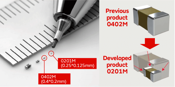 Figure 2. Appearance of MLCCs of size 0402M and 0201M
To date, Murata has been leading the world in miniaturization of MLCCs and has been contributing to the miniaturization of electronic devices. The 3216M (3.2 x 1.6 mm) size MLCC introduced in the 1970s was used to develop compact and thin portable radios, and the 2012M (2.0 x 1.2 mm) and 1608M (1.6 x 0.8 mm) sizes were introduced in the 1980s and 1990s to make AV equipment and PCs smaller and more portable. In the 2000s, the 1005M (1.0 x 0.5 mm) and 0603M (0.6 x 0.3 mm) sizes helped to make cell phones (feature phones) more multifunctional. Because of this record of accomplishment of proactive efforts to reduce the size of MLCCs, we have captured more than 50% of the market share of 0402M size MLCCs, which are widely used in smartphones.
At Fukui Murata Manufacturing, a mass-production system is already in place for the 0201M size, 0.1 μF MLCC developed for use in 5G-enabled smartphones. Going forward, Murata will continue to lead the way in miniaturization of MLCCs and to support the miniaturization of electronic devices as well as greater multifunctionality and higher performance.
Reducing the Size of the Numerous MLCCs in Devices to 1/5
A single 5G-enabled smartphone contains a large number of MLCCs. This component has a significant impact on the miniaturization of the device. The miniaturization of MLCCs is essential for making devices multifunctional while maintaining a usable size. Over the past nearly half century, Murata has been a leader in the miniaturization of MLCCs. And building on our past achievements, we have developed a new generation of compact MLCCs that are designed for installation in 5G-enabled smartphones. We asked the product planners of MLCCs for 5G-enabled smartphones and the engineers who have been working on the development of smaller and higher capacitance MLCCs about the details of the MLCCs they have developed and their impact on device development.
With More Than 1,000 MLCCs Used per Device, Their Miniaturization Has a Significant Impact
For what applications and how many MLCCs are used in 5G-enabled smartphones?
Today’s smartphones are rapidly becoming more and more multifunctional. In addition to the electronic circuits for wireless communication, smartphones include many other electronic circuits, such as displays, cameras, and processors for executing a wide range of processes. To ensure stable operation of these electronic circuits, many capacitors are used to supply power and eliminate noise.
Smartphones need to pack a lot of electronic functions into a small chassis, and the capacitors need to be as small as possible. For this reason, most of the capacitors used in smartphones are MLCCs, which excel in miniaturization, and there are now more than 1,000 MLCCs in each high-end, state-of-the-art smartphone.
There are so many MLCCs being used, it may be the most widely used component in smartphones. So, what characteristics of MLCCs are required for 5G-enabled smartphones?
MLCCs with smaller size and larger capacitance are needed. 5G-enabled devices are expected to have more functions installed in a single unit than 4G devices, and as a result, the electronic circuits installed in the chassis are expected to be larger. This will further increase the number and total capacitance of MLCCs in the device (Figure 3).
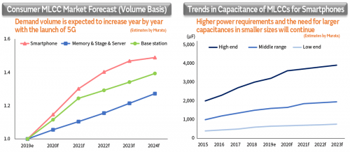 Figure 3. Market forecast for consumer MLCCs and MLCC capacitance in smartphones
For example, 5G devices will need to support more frequency bands than 4G devices. In order to provide high-quality communications while using various frequency bands within a single device, the noise mixed from unused frequency bands must be removed by filtering out the frequency bands that are not used. In these devices, many MLCCs are used that have small capacitance but low capacitance variation.
However, it is becoming increasingly difficult to even maintain the current size of the smartphone chassis, and there are growing needs to make it smaller. To meet these needs, further miniaturization of MLCCs is essential.
Battery capacities are also increasing due to the added functionality of devices. In order to charge large-capacity batteries stably and quickly, higher capacitance and higher quality MLCCs are needed. Furthermore, demand for higher capacitance MLCCs remains strong because, in certain electronic circuits, the number of MLCCs can be reduced by using higher capacitance products.
1/2 the Mounting Area and 1/5 the Volume Compared to the Same Capacitance Product
What features did Murata develop in its MLCCs for 5G-enabled smartphones in order to increase the scale of circuits and maintain or reduce the size of devices?
By introducing a new generation of manufacturing technology, we have developed the world’s largest capacitance MLCC of 0.1 μF in the 0201M size, which is the smallest MLCC size currently available. MLCCs in the 0201M size have been available in the past, but their small capacitance of 0.01 μF limited their use in smartphones. Furthermore, we have achieved a product with a rated voltage of 6.3 V and a capacitance tolerance of ±20%, which is suitable for smartphones.
Before, MLCCs of the same capacitance, which have been used in many smartphones, were 0402M in size. This has been reduced to 0201M size, which uses only 1/2 the mounting area and 1/5 the volume, making it significantly smaller. In addition, we have also developed a 0402M size 1.0 μF MLCC using the new manufacturing technology that we adopted for this MLCC. This one also has the world’s largest capacitance for MLCCs of the same size.
What impact will the MLCCs that you developed have on the development of 5G-enabled smartphones?
I mentioned earlier that more than 1,000 MLCCs are used in the most advanced smartphones. More than 200 of them correspond to the 0.1 μF and 1.0 μF products that we developed this time. Since each of these MLCCs has been dramatically reduced in size, this will have a tremendous impact on the miniaturization of devices.
The MLCCs that we have developed will enable development of devices with higher added value by allocating the space saved from the reduced substrate area to add further functions and higher battery capacity. In addition, wearable devices and IoT devices have higher added value because of their small size. Smaller wearable devices are less uncomfortable to wear, which expands their usage scenarios. Smaller IoT devices are also more likely to collect valuable data because the requirements for installation locations are relaxed. Therefore, we believe that the newly developed MLCCs will be widely used in these types of applications.
You mentioned that the rated voltage is 6.3 V, but what does that mean?
The battery in a smartphone provides power at 3 V to 4 V. Therefore, an MLCC rated at 6.3 V is an easy specification to use in electronic circuits that are directly driven by that battery. In smartphones, some components such as processors are driven at about 1 V, where MLCCs rated at 4 V are often used. However, some customers also use MLCCs rated at 6.3 V for circuits around the processor to reduce the complexity of parts management. For this reason, it is important to have the smallest size product available with a 6.3 V rating.
Ready for Mass Production
When and where will you start mass production of MLCCs developed for 5G?
A mass production system is already in place, and mass production is scheduled to begin at Fukui Murata Manufacturing in 2020. Within the Murata Group, Fukui Murata Manufacturing is our flagship plant that leads the way in developing miniaturization and larger capacitances for MLCCs in terms of both technological development and mass production (Figure 4). It is responsible for being the first to adopt new technologies for cutting-edge miniaturization and larger capacitances and for transferring the technologies to other production bases when the technologies mature.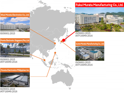
Figure 4. Murata’s main MLCC production sites
For the widespread use of compact MLCCs, customer companies will need state-of-the-art mounting machines (mounters) that can handle the mounting of small electronic components. The 0201M size is extremely small, but we started mass production in April 2014. At that time, we completed the development of the corresponding mounter with the mounter manufacturer, and our customers were ready to use this size MLCC. With the production of 5G-enabled smartphones in full swing, demand for 0201M size is rapidly growing, and we are confident that demand will increase in the future.
MLCCs Are Difficult to Miniaturize While Increasing the Capacitance
At what pace will MLCCs become smaller and have larger capacitances due to advances in manufacturing technology?
In the past, MLCCs with the same capacitance have progressed in a cycle of about 7 to 10 years when compared to each other.
Semiconductor microfabrication and manufacturing technologies are renewed every two or three years, with the 14 nm generation, 10 nm generation, and 7 nm generation. In comparison, the miniaturization of MLCCs seems to be progressing more slowly. What are some of the difficulties in miniaturizing and increasing capacitance?
Electronic component manufacturers cannot simply leap ahead in the miniaturization of MLCCs. This is because as the size of components becomes smaller, user companies will need to establish new mounting technologies to use them. For example, mounters (mounting machines) that mount components on printed circuit boards to be incorporated into electronic devices need to be improved to support small electronic components and to improve mounting accuracy. For this reason, the miniaturization of MLCCs must move in tandem with the evolution of mounting technology.
In addition, MLCCs have technical difficulties that differ from those of semiconductor miniaturization in achieving smaller size and larger capacitances. MLCCs have a structure consisting of alternating layers of thin dielectric ceramic sheets and metal electrodes (Figure 1). A slurry of ceramic dielectric and binder that is coated on a carrier film and dried is called a green sheet, and electrodes are printed on this green sheet repeatedly before being baked and hardened. In modern MLCCs, the number of layers can be several hundred. A particularly difficult aspect of MLCC manufacturing is that the ceramic sheet shrinks significantly after sintering. If the dielectric film and electrodes are simply made thinner, the entire film may crack due to shrinkage during sintering. In order to create the desired element structure after sintering with the electrode pattern printed, appropriate technology and expertise are required.
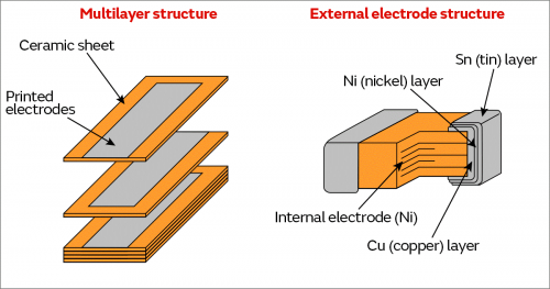
Figure 1. Basic structure of MLCC
The technology used in the manufacture of our newly developed products enables a thickness of the ceramic sheet that is only 1/100th of the thickness of a hair (about 80 μm). In order to produce high-quality MLCCs with high yield, the film thickness of the thin ceramic sheet must be made uniform. If the film thickness is not uniform, the electrodes that sandwich the dielectric sheet may touch and short circuit. If this happens, it will not function as a capacitor. Even if there is no short circuit, large variations in film thickness can lead to lower withstand voltage and reduced reliability.
Developing Cutting-Edge MLCCs through Integration and Coordination of Raw Material Development and Manufacturing Process Development
You need a considerably high-precision manufacturing technology to create MLCCs that meet your requirements. Specifically, what kind of manufacturing technology did you develop to create the most advanced MLCCs with 0.1 μF in 0201M size and 1 μF in 0402M size?
The quality of the raw materials needed to be higher than ever before. First, we made the dielectric (barium titanate) particles finer in size and uniform in variation to produce a homogeneous and dense green sheet. At the same time, we developed a technology to form fine dielectric particles by dispersing them evenly in a thin sheet. In addition, the particle size of the metal (nickel) particles used to print the electrode pattern has been made finer. The filling ratio has been improved so that large bumps do not occur at the interface between the electrode and the dielectric even when the layer is thin.
The process of miniaturization and higher capacitance for MLCCs must begin not simply from development of manufacturing processes, but also from the development of raw materials.
That’s right. Improving and optimizing the manufacturing technology by coordinating both the material and sheet forming technologies together is a key point for miniaturizing and increasing the capacitance while ensuring a high level of quality and reliability. Therefore, unless a company can develop both materials and manufacturing processes in-house, it will not be able to lead the way in miniaturizing and increasing the capacitance of MLCCs.
Murata’s tradition of developing and manufacturing products in-house from raw materials has continued since the company’s founding. Moreover, we do not simply develop and produce raw materials in-house; we have a system in place that allows each department, including production engineering, product planning, and sales, to work together to create the raw materials necessary to realize the required products and maximize their potential. In some cases, we can find solutions to difficult-to-resolve issues with raw materials by using a little ingenuity in the manufacturing process. This ability to create new technologies and products from raw materials across the organization is one of Murata’s strengths, and I believe it is the reason that we have been able to gain a high market share in the MLCC market.
I understand that you are doing cross-organizational development, but do you have a development environment that facilitates cross-departmental collaboration daily?
The development and mass production functions for state-of-the-art MLCCs are integrated in Fukui Murata Manufacturing. Here, we have accumulated advanced technologies and a wealth of experience and expertise related to thinning and layering. And since the development, production engineering, and manufacturing departments are all located in the same place, experts in each field can easily convene for active communication under the leadership of product development. We believe that this CFT (Cross Function Team) development system has led to the speedy development of our technology.
In addition, the fact that we are developing technology in a place where there is a mass-production plant nearby has the effect of enabling us to quickly bring world-leading technology to mass production. Technological development that only involves thinking at the desk will not solve the problems that occur at the manufacturing site. It is extremely important for the engineering and manufacturing departments to work together to find solutions while actually observing the situation on site.
The development department alone cannot tackle difficult technical issues such as miniaturizing and increasing the capacitance of MLCCs. Thanks to the cooperation of the production engineering, manufacturing, and sales departments, we have reached a state where we can mass produce the world’s first product (Figure 2). I am very grateful to those who faced the difficulties with us and helped us find solutions.
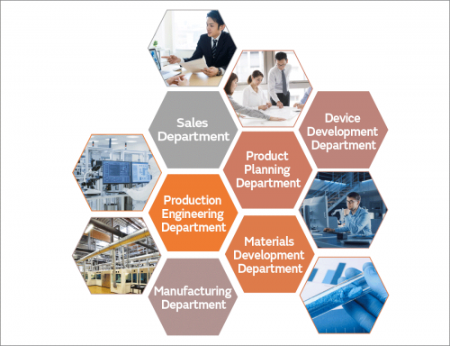
Figure 2. Collaboration system for developing new MLCCs
Preparations for Further Miniaturization and Higher Capacitances Are Already Under Way
The demand for smaller and more multifunctional electronic devices, not just smartphones, will continue to grow. Will Murata continue to rise to the challenge of further miniaturizing and increasing the capacitance of MLCCs in the future?
We have been taking on the challenge of developing technologies to make MLCCs smaller and with higher capacitance since before the demand for further miniaturization even became apparent. And as a result, I believe that we have been able to contribute to the evolution of electronic devices. Currently we are not working on developing MLCCs smaller than 0201M size. However, we are continuing to work on further thinning of the dielectric and electrodes and will surely start further miniaturization of the MLCC.
Technologically, is there still room to make MLCCs even smaller and larger in capacitance?
We see a path to further miniaturizing the dielectric particles used as raw materials, and we already have the technology to form even thinner sheets.
We have also been able to make the electrodes even thinner by pushing forward with the miniaturization of the nickel particles that make up the electrodes. In the future, by combining and coordinating both sides, we will establish next-generation manufacturing technology to develop smaller and larger capacitance MLCC products.
We are already starting to hear about the development of 6G technology. How do you see the MLCCs for developing applied devices with 6G?
It is said that 6G will be put into practical use in 2030. It is said to be a high-speed communication with even lower latency than 5G, and we believe it will bring significant changes in the functions and usage scenarios of smartphones and wearable devices. For example, we may see the development of applications with keywords such as “remote control.” In this context, what MLCC manufacturers need to do is to reduce the size and increase the capacitance. Over the next three to five years, the required technologies will gradually become clearer. We will continue to be one step ahead in developing technologies so that we can respond quickly to the situation.
Also Supporting the Miniaturization of Wearable Devices and IoT Devices
Murata’s MLCCs are used in most smartphones on the market today. This is because only high-performance MLCCs can meet the needs of consumers for smartphones and overcome the difficult technological hurdles. This trend will become even more pronounced with the introduction of MLCCs for 5G-enabled smartphones that incorporate a new generation of manufacturing technology.
MLCCs developed for 5G-enabled smartphones are also likely to drive the evolution of other electronic devices, such as wearable devices and IoT devices. In the background of the rapid evolution of electronic devices, there has always been innovation in the electronic devices that support them. Examples include the invention of the microprocessor, which led to the creation of the personal computer, and the evolution of LCD panels, which facilitated the commercialization of flat-screen televisions. It will be interesting to see what kind of innovative electronic devices will be created by the new generation of MLCCs.