


There are two kinds of transient responses. First, Load Transient Response is when there is a change of load current provided by the LDO (linear dropout) regulator, overshoot or undershoot occurs at the LDO output. Second, Line Transient Response is when a change of connected voltage is at the LDO input, overshoot or undershoot happens at the output in a different shape.
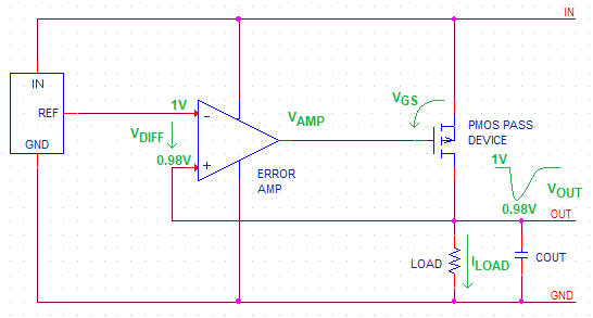
Let’s look at what happens inside the LDO when an undershoot appears at its output. Figure 1 shows an LDO internal structure with an output voltage of 1 V and Transient Response undershoot of 0.02 V, resulting in an output voltage drop to 0.98 V. When the reference voltage stabilizes to 1 V, then there is a voltage difference of 0.02 V between the inputs of the error amplifier. The amplifier amplifies that voltage, so the output voltage of the error amplifier VAMP decreases, meaning the VGS of the PMOS pass device increases, and the PMOS pass device starts to open its channel more to charge the output capacitor. So, the output voltage of the LDO starts to increase back to 1 V.


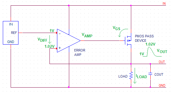
The case of overshoot at the output of LDO (Figure 2) is the opposite of the undershoot situation. Overshoot is 0.02 V, so the output voltage is 1.02 V. There is a voltage difference of -0.02 V between the inputs of the error amplifier. The error amplifier amplifies this voltage again, and the output voltage of the error amplifier VAMP increases while the voltage VGS of the PMOS pass device decreases, meaning the PMOS pass device starts to close its channel. But just because of that, one pass device can charge the output capacitor in case the overshoot output voltage returns to 1 V when the output capacitor discharges.
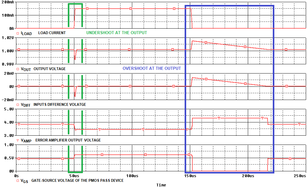
You can see the Load Transient Response and described action inside the LDO during undershoot and overshoot in Figure 3: the pass device opens more during undershoot and closes during overshoot. This feedback action is the same for Load Transient Response and Line Transient Response, but it depends on what causes the undershoot or overshoot. The amplitude of overshoot and settling time depends on how fast the internal feedback can react to the transient event—any change of input voltage or load current.
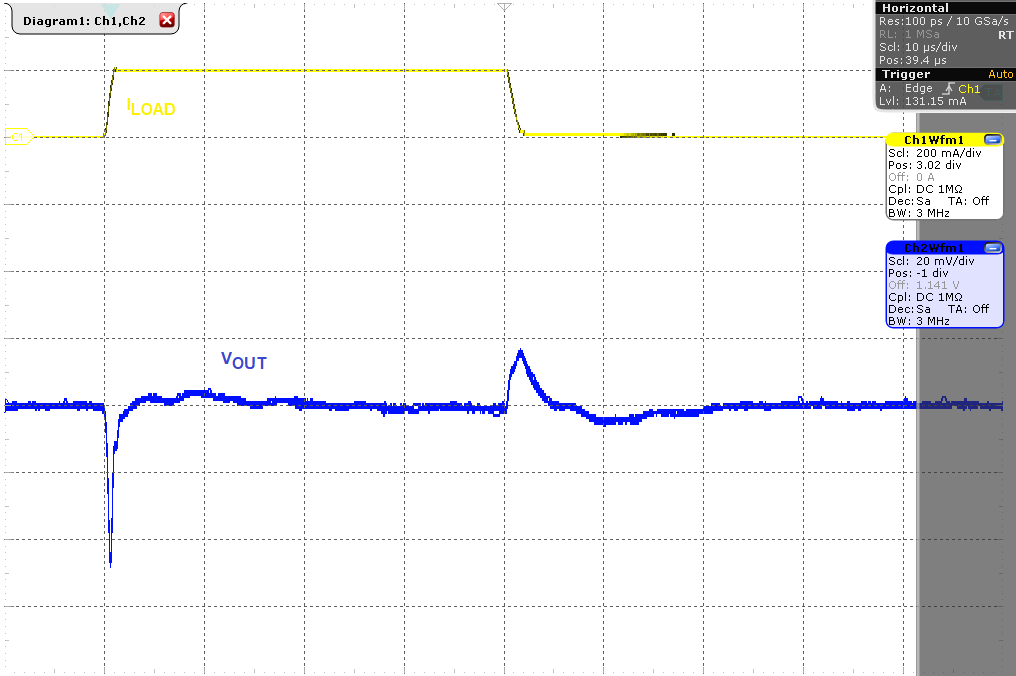
Figure 4 shows the measured Load Transient Response of NCP110: the output voltage drops during load change to a higher current level. After some time, the internal feedback reacts to the undershoot and opens the PMOS pass device. When the load changes to a very low current level, for example, 1 mA, the internal feedback responds by closing the PMOS pass device: overshoot results, and the output capacitor discharges.
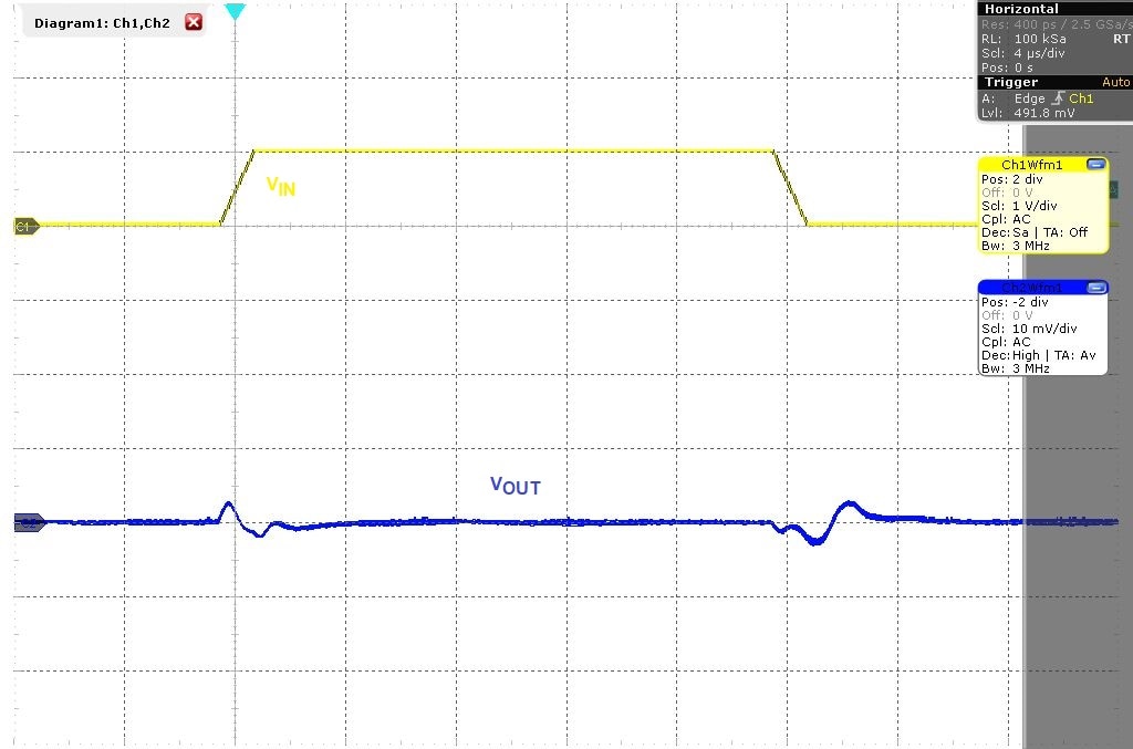
Figure 5 shows the Line Transient Response. But undershoot and overshoot have the same shape—caused by the fact that there is no change in the load current. So, there is no extended discharge of the output capacitor. Like the Load Transient Response, the PMOS pass device opens and closes in response.
You can apply a similar principle to the LDO with an NMOS pass device. The LDO with a PMOS pass device has a Gate-Source voltage VGS orientated against the input voltage VIN, and the LDO with an NMOS pass device has a Gate-Source voltage VGS orientated against the output voltage VOUT. So, when there is a need to open the NMOS pass device more, the output voltage VAMP of the error amplifier increases. When there is a need to close the NMOS pass device, the output voltage VAMP of the error amplifier decreases; it is precisely the opposite of the LDO with a PMOS pass device.
Authored Article by: Pavel Vlcek, Onsemi