


No, you can adapt a unipolar gate driver to drive in a bipolar manner.
If a positive and negative gate drive is required for a particular power device, circuit designers don’t need to search for a special gate driver that handles bipolar operation specifically. Use this simple trick to make a unipolar gate driver deliver bipolar voltages!


When driving medium to high powered MOSFETs and IGBTs, there is a risk of a Miller effect induced turn-on when a high rate of change of voltage is seen across the power device. Current is injected onto the gate of a power device through the gate-to-drain or gate-to-collector capacitance. If the current injection is large enough to bring the gate voltage above the device threshold voltage, parasitic turn-on can be observed resulting in lower efficiency or even device failure.
The Miller effect can be mitigated through use of a very low impedance path from the power device gate to the source or drain, or by driving the gate to a negative voltage with respect to the source or drain. The goal of the Miller effect turn-on mitigation techniques is to keep the gate voltage below a desired threshold when a current spike through the Miller capacitance occurs.
Certain power device types even require a negative voltage to be fully off, necessitating some kind of negative voltage drive coming from the gate driver. Device manufacturers that recommend negative gate drive voltage include standard silicon MOSFETs, IGBTs, SiC, and GaN devices.
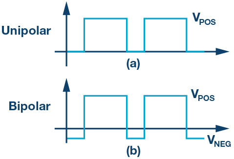
There is a wide selection of isolated gate drivers that operate on a unipolar power supply on the secondary side (the side driving the power device), but much fewer gate driver devices that allow for explicit bipolar voltage drives. One method to overcome this lack of negative gate drive devices is to offset the gate driver from the power device, thereby creating a negative gate drive relative to the source or drain of the power device, while the gate driver IC still only sees a unipolar supply. Unipolar and bipolar gate drive waveform examples are shown in Figure 1.
A schematic with ideal voltage sources pictured is shown in Figure 2. In this example, the driver IC is powered by a voltage equal to the sum of V1 and V2, while the gate of the MOSFET is driven to a +V1 in the ON state and a –V2 in the OFF state, relative to the MOSFET source node. Note that in this example, both voltage sources are decoupled with individual capacitors. The effective decoupling seen by the gate driver IC is the series combination of the capacitors, which is less than the value of each individual capacitor. Additional decoupling can be added between VDD and GND if desired, but it is important to keep C1 and C2 as the capacitors provide low impedance paths for the gate current during turn-on and turnoff separately.
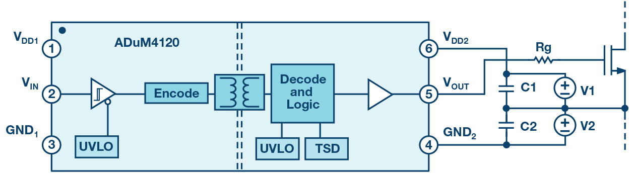
Isolated gate driver ICs often come with an under voltage lockout (UVLO) to prevent a power device from being driven weakly if the gate driver is being driven with too low of a gate voltage. When driving a unipolar gate driver as shown in Figure 2, care must be taken with the expected operation of the UVLO as the UVLO is usually referenced to the ground of the gate driver. Consider a case where V1 = 15 V, V2 = 9 V, and the gate driver UVLO is around 11 V, which is common for IGBT operation. If V1 were to drop more than 4 V, the UVLO would not trigger, but the IGBT would be driven under 11 V during the ON time, thereby under driving the IGBT.
Creating two separate voltage sources for this purpose can be accomplished by using two isolated power supplies, but cost is often a concern for this approach. If a flyback topology is used, multiple winding taps could be used to obtain multiple voltages relatively easily.
There are isolated voltage source modules that can provide isolated power, and some manufacturers are selecting voltages conducive to power device voltages. One example is RECOM, with devices such as the IGBT targeted product line that produces an isolated +15 V and –9 V rail.
For such a large voltage swing, the gate driver must be able to withstand a larger range than the range at which other devices were targeted. Two gate drivers that work well with these voltages are ADI’s ADuM4135 and ADuM4136 IGBT gate drivers with iCoupler® technology, which have a recommended voltage range that allows up to 30 V. Both provide a dedicated ground pin on the output side, allowing the driver UVLO to be referenced against the positive supply rail. The ADuM4135 also includes an integrated Miller Clamp, which can further help suppress the Miller induced turn-on gate voltage bump.
A simple method for creating a bipolar supply from a single voltage source is to create a second voltage source using a biased Zener diode. Although gate drivers provide high currents during the turn-on and turn-off of a power device, the average current actually needed from the power supply is relatively low—often in the tens of mA range for most applications.
The Zener diode can be placed to either regulate the positive or the negative voltage, and can be selected based on which rail needs higher accuracy. The example shown in Figure 3 is setup to regulate the positive voltage more than the negative voltage. One reason to regulate the positive voltage could be if the gate being driven has a tight tolerance on the gate voltage requirements, such as in the case of some GaN devices. Regulating the positive supply also has the added benefit of allowing the UVLO of the gate driver to act as expected, since any fluctuation in V3 will be attenuated by the Zener diode until V3 is too low to support the Zener voltage.
Using the Zener diode method to create two supplies out of a single supply also has the benefit of layout savings. Not only does a Zener diode and a resistor effectively replace an entire isolated voltage source, but by using a unipolar isolated gate driver, a six pin device can be used, such as ADI’s ADuM4120 with iCoupler technology—saving even more space around the gate driver IC along the isolated creepage area.
A reference example of the Zener diode bipolar setup was created using ADI’s ADuM4121 and GaN Systems’ GS66508T to create a half bridge. The example was designed to have a +5 V and –4 V drive referenced to the device source. The example could easily be adapted to have +6 V and –3 V drive by using a different Zener diode, and the same 9 V isolated power supply. A large dead time is used to separate the Miller bump from other turn-off transients visually, but in practice the ADuM4121 allows for much shorter dead times in the tens of ns range, which is an important