


The need for high performance in the CPU VR (voltage regulator) world has been with us for a few years now, but increasingly the PoL market is now under pressure to meet stricter requirements.
No longer is the mighty CPU the only power hungry silicon on the board. Today’s ASICs are drawing in excess of 100 W and are requiring sophisticated features such as dynamic voltage changes/ AVS, margining, autonomous phase shedding, telemetry, PMBus compatibility, tight output voltage accuracy under demanding transient conditions, and high efficiency under light loads. Once only the realm of the CPU, the ASIC is moving center stage in demanding a high performance VR.


Integrating the IR product portfolio, Infineon now offers a variety of end to end solutions. For single phase fully integrated packages (controller/driver/MOSFETs) there are ten parts available ranging from the 3 A IR3823, to the 35 A IR3846. The SupIR product line continues with dual output 4 A + 4 A and 6 A + 6 A fully integrated solutions.
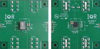
As a result of a new thermally enhanced package using copper clip and several proprietary innovations in the controller, the SupIRBuck family can operate up to 35 A without a heatsink, and reduces PCB size by 20 percent compared to alternative integrated solutions and 70 percent compared to discrete solutions using a controller and power MOSFETs. A complete 25 A power supply solution can be implemented in as little as 168 mm2 as shown in Figure 1.
The devices integrate a feature-rich, third generation SupIRBuck controller that includes post-package precision dead-time trimming to optimize losses, and internal smart LDO to optimize efficiency across the entire load range along with the power MOSFETs. True differential remote sense essential for high current applications, 0.5 percent reference voltage accuracy in 25 °C to 105 °C temperature range, input feed-forward and ultra-low jitter combine to enable total output voltage accuracy less than 3 percent over line, load, and temperature, as required by high performance communications and computing systems.
The third generation SupIRBuck single input voltage (5 V – 21 V) family features a proprietary modulator scheme that reduces jitter by 90 percent compared to standard solutions. This has the dual benefit of reducing output voltage ripple by approximately 30 percent and allowing higher frequency (up to 1.5 MHz) and higher bandwidth operation for smaller size, better transient response and fewer output capacitors. To aid in ease of use, an online design toolkit provides a part selection matrix, simulator, and schematic/BOM generation.
The lineup extends to the high performance fully digital multiphase controller family which is based on a highly reliable state machine core that delivers performance and flexibility from single phase single loop devices, three phase three loop devices, and even to an eight phase single loop device. All parameters of the controller are set via firmware that is stored in non-volatile memory. Accessible over I2C and PMBus, the system engineer is able to adjust all parameters of operation in real time without the need to interrupt active regulation. System parameters such as number of phases, switching frequency, frequency response, dynamic voltage change, and numerous fault and protection features (OCP, OOVP, OUVP, etc.) can all be adjusted by firmware.
A unique feature of the PXP1000 series controllers is the embedded microcontroller. The intention of the microcontroller is to offer virtually unlimited flexibility in the control of the regulator, as well as the ability to add new functionality on the fly as requirements develop during the design process.
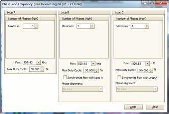
Using a dedicated GUI the designer has a simple interface to control all the parameters of the controller. A few clicks set up the turn on conditions for features like Vin OVP, UVP, UVLO and even an input current monitor. Also software adjustable are the number of phases and switching frequencies, which are fully flexible for each loop (or independent output) as shown in Figure 2.
The controller features a PID compensation loop that is similar to an analog regulator’s type III compensator. Independent PID loops for each output, and even each power state (i.e. dynamic phase count applications) allows the ability to keep transient performance optimized under all load conditions.
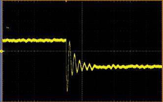
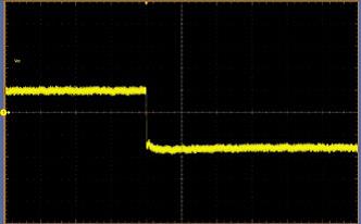
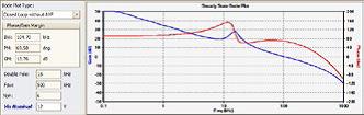
Figure 3 depicts the VR response to a high current step load. As is clearly evident, without controller adjustments the output is highly unstable (Fig. 3a). After making a few adjustments to the PID loop parameters (while in active regulation), the response has been optimized and no undershoot or ringing is observed (Fig. 3b). Of note, this particular application has droop (loadline) so the step response should be a square wave.
The built in Bode plot simulator allows the modeling of the board’s output stage by entering inductor value, bulk capacitors as well as larger caps near the load, and even PCB parasitics. Once the board is simulated, the GUI can recommend stable PID parameters for all loops. The GUI also features a poles and zeros translator for conversion into PID parameters. The simulator and P&Z converter ease the transition of the designer from the analog world to the digital world of power.
If the response of the loop is not adequate due to a board layout issue, or limited capacitor bank, the advanced features of the digital controller can be of great help. Many non-linear response parameters are available to overcome difficult operating conditions. During a load step increase, the Automatic Transient Response feature inserts extra PWM pulses to drive more current into the load. All while ensuring that inductor saturation limitations, on a phase by phase basis, are never exceeded, even under stressful thermal conditions. During a load step release, the PWM pulses are automatically blanked, if additional performance is required the controller can tri-state the power stage to dissipate energy in the low side body diode thereby reducing the output voltage. The controller features sophisticated limits to protect the power stage from over current during this and all operating conditions.
The output voltage is firmware programmable, as is the droop or loadline (AVP) setting. During active regulation the output voltage is adjustable by programmable VID settings. The controller features a flexible architecture that allows many different VID schemes that are dependent on the application. Output regulation is maintained within 0.5 percent of the desired setpoint, and a sophisticated fault handler watches for output voltage over threshold, under threshold, and VID tracking threshold errors. Even when the fault handler detects an error, the firmware has an adjustable response to the errors, which is extremely useful during bench debug or testing. The controller also supports PMBus so margining and other commands are readily accessible over the I2C bus.
Extremely valuable is the vast amount of telemetry data that is avail- able via I2C or PMBus. Output voltage, high accuracy output current (both per phase and total), power stage temperature, controller tem- perature, input voltage, and input current offer a wealth of information that is useful during debug and during normal operation. Over I2C a system monitor can read the information and make decisions about the health of the controller and/or system.
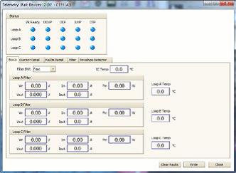
This information can then be sent up the chain to chassis or rack system monitors for constant supervision of the health and status of the power delivery system. The ability to detect abnormal operating conditions before they become major problems is helpful in maintaining system up time. Because the system communication is two-way, the ability to modify control parameters in deployed systems is also available. The telemetry data also available in the GUI is shown in Figure 5.
(Design article courtesy: Infineon Technologies)