


Courtesy Infineon technologies
Clamping circuits are sometimes used in IGBT drive circuits. The main purpose is to protect IGBT devices and prevent operating parameters from exceeding the limit parameters of the collector or gate. Today we summarize the precautions for the design and use of Vce and Vge clamping circuits.


Vce clamp circuit
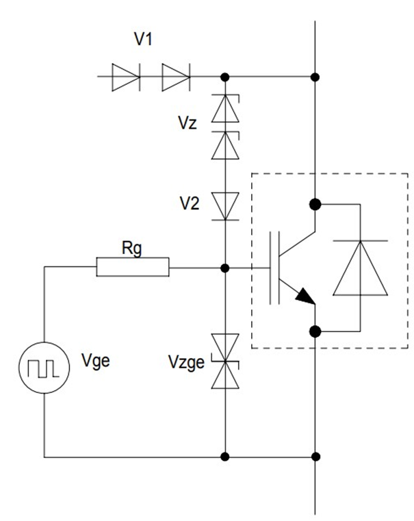
The purpose of the Vce clamp circuit is to prevent the peak voltage between Vce from exceeding the maximum value that the device can withstand under special working conditions such as high current, short circuit, and low temperature. The basic structure of the circuit is shown in the figure below. This circuit is adopted by many designers because of its simple design and immediate effect.
The selection of its clamping voltage can use the following formula:
in:
![]()
- Vmax is the maximum value of Vce voltage allowed in the circuit design, and the blocking voltage of the device and the margin should be considered
- Vz is the rated voltage of the clamping diode
- aT is the temperature drift coefficient, usually 0.1%, the specific value needs to refer to the data sheet of the selected device
- Tj is the actual operating temperature of the device
- Tv is the tolerance of the clamping voltage value of the device, for example, 5% or 10%, please refer to the device data sheet for the specific value
Vce peak is the device blocking voltage
However, there are also two completely different views on this circuit. One view is that due to the great influence of the clamping diode tolerance and temperature drift, the voltage value of the on-on voltage varies greatly during actual operation, resulting in the clamping voltage. fixed, so it is not used in actual design; another point of view is that this kind of circuit is relatively simple to implement, even if the characteristics of the diode are not very stable, but the redundancy is appropriately increased or multiple diodes with lower clamping voltage are connected in series, it can also achieve The purpose of reducing the tolerance of the clamping diode, so that the deviation of the clamping voltage value is relatively reduced. The two design ideas have their own advantages and disadvantages. Which one would you consider?
Vge clamp circuit
In the design of the IGBT drive circuit, three methods can be used to control the voltage between Vge within the allowable range of the device.
The first type uses a bidirectional clamping diode between VDZ and GE in Figure 2;
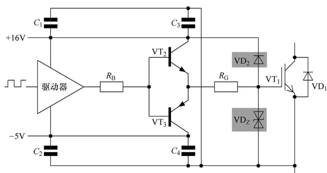
The second one connects the gate to the drive power supply through a fast diode (VD2 in Figure 2);
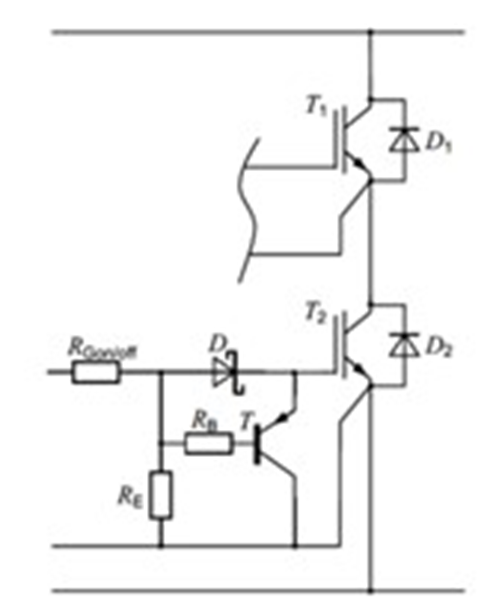
The third is to use a triode between GE to pull down the gate voltage to the emitter (as shown in Figure 3).
First look at the use of bidirectional clamping diodes between GE . This circuit can effectively reduce Vge voltage spikes, so as to ensure that the voltage of Vge remains at the voltage level expected by the designer in certain occasions such as a short circuit. However, in many years of practical application practice, the author found that bidirectional diodes will undergo unidirectional breakdown after long-term operation, and unilateral failure will appear in a short circuit state. Please pay special attention to the design and use.
The second design is to connect to the positive power supply of the drive through a Schottky diode in the Vge circuit, such as the diode VD 2 in Figure 2 above . This circuit is actually a simplified design of the first circuit above. Due to the working characteristics of the circuit, the negative voltage in the drive circuit is relatively stable, which can be solved by power supply design, and the positive voltage will pass through the current of the Miller capacitor when dudt changes. Raise the gate voltage, so a clamping circuit is needed to clamp the positive gate voltage at an appropriate position, such as a +15V drive power supply. When choosing a diode, consider the withstand voltage of 40V. In addition, if the package allows, choose a device with a slightly larger average current, so that in practical applications, the voltage drop is small and it is easier to clamp the voltage at a level close to the positive power supply. At the same time, the diode should be close to the gate when wiring.
The third circuit is also called Miller clamp, which is mainly used when the gate turn-off voltage is 0V, and is often used in some low-power occasions. When the pair is turned on, the change of udt will raise the gate voltage of the other IGBT which is in the off state. Under certain conditions, the IGBT devices in series will be turned on at the same time, resulting in a short circuit. In order to avoid this situation, the Rb+T circuit shown in Figure 3 can be used. When the IGBT is in the off state, the Vge voltage is at a low level, such as 0V, so the transistor T is in the on state. When wiring, ensure that the triode is placed close to the gate of the IGBT to ensure that the gate voltage level of the IGBT is at a pull-down level, thereby providing a low-impedance loop for the Miller current, and avoiding the gate voltage level being affected by the Miller current.
Summarize
- Gives the calculation reference for Vce active clamp circuit diode selection, but whether to choose this circuit depends on the designer’s design tendency and risk assessment.
- There are three types of Vge clamping circuits:
- Use bidirectional clamping diodes, but there will be unilateral failure problems during use, so use them with caution;
- Connect the gate +15v to the positive pole of the power supply through the Schottky diode to achieve the clamping effect;
- When the gate turn-off voltage is 0V, a low-resistance circuit is set between the gate and the collector through the triode to avoid parasitic conduction caused by the Miller voltage.