


Introduction
The MAX1606 is a step-up DC-DC converter that contains a 0.5A internal power switch and a 0.5A output isolation switch in an 8-pin µMAX package. The IC operates from a 2.4V to 5.5V supply voltage but can boost battery voltages as low as 0.8V up to 28V. The MAX1606 uses a unique control scheme that provides high efficiency over a wide range of load conditions. An internal 0.5A MOSFET reduces external component count, and a high switching frequency (up to 500kHz) allows for tiny surface-mount components. The current limit can be set to 500mA, 250mA, or 125mA, allowing the user to reduce the output ripple and component size in low-current applications. Additional features include a low quiescent supply current and a true shutdown mode that saves power by disconnecting the output from the input. The MAX1606 is ideal for small LCD panels with low current requirements, but can also be used in other applications.


Main features include the following:
- Adjustable Output Voltage Up to 28V
- 20mA at 20V from a Single Li+ Battery
- True Shutdown (Output Disconnected from Input)
- Output Short-Circuit Protection
- Up to 88% Efficiency
- Up to 500kHz Switching Frequency
- Selectable Inductor Current Limit (125mA, 250mA, or 500mA)
- 1µA Shutdown Current
- 8-Pin µMAX Package
Hardware Specification
A single-output boost converter using the MAX1606 is demonstrated for a 1V to 3.3V input voltage range. The output is configured to be equal to 13.5V. The power supply delivers up to 6mA at 13.5V with up to 4% output voltage regulation at 1V. Table 1 shows an overview of the design specification.
Designed–Built–Tested
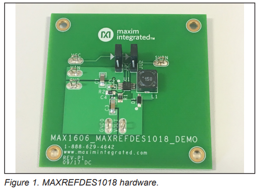
This document describes the hardware shown in Figure 1. It provides a detailed systematic technical guide to design in a boost converter using Maxim’s MAX1606 current-mode, step-up DC-DC converter. The maximum efficiency of MAX1606 is up to 88%, however, this document describes a design that can turn on at a low input voltage of 1V and deliver at least 6mA load current with reasonable regulation. The emphasis is on power delivery rather than on efficiency. The benefit of the MAX1606 lies in its simple design and lowest component count, with internal compensation and high efficiency at nominal input voltages. The power supply has been built and tested, details of which follow later in this document.
Table 1. Design Specification
| PARAMETER | SYMBOL | MIN | MAX |
| Input Voltage | VIN | 1V | 3.3 V |
| Frequency | fSW | 500 kHz ( variable ) | |
| Output Voltage | VOUT | 13 .5 V | |
| Output Current | IOUT | 0A | 6 mA |
| Maximum instantaneous
Output Power |
POUT | 81 mW at 1V | |
The board can be operated from a single power supply. To evaluate the board with a single supply, connect a jumper wire from the VIN pad to the VCC pad. Connect a +2.4V (min) to +5.5V (max) power supply to the VIN or VCC pad. There are two jumpers (JU1 and JU2) on the board that can be configured as shown in Table 2 and Table 3.
Design Procedure for Boost Converter Design Using MAX1606
The MAX1606 features a minimum off-time, current-limited control scheme as shown in Figure 2. The duty cycle is governed by a pair of one-shots that set a minimum off-time and a maximum on-time. The switching frequency can be up to 500kHz and depends upon the load and input voltage. The peak current limit of the internal n-channel MOSFET is pin selectable and can be set at 125 mA, 250mA, or 500mA.
Table 2. Jumper JU1 Options
| SHUNT LOCATION | LIM PIN | INDUCTOR CURRENT LIMIT (mA) |
| 1 and 2 | Connected to VCC | 500 |
| 2 and 3 | Connected to GND | 125 |
| None | Floating | 250 |
Table 3. Jumper JU2 Options
| SHUNT LOCATION | SHDN PIN | OUTPUT |
| 1 and 2 | Connected to VCC | ON, VOUT = +13.5V |
| 2 and 3 | Connected to GND | OFF, VOUT = 0V |
Step 1: Setting Output Voltage
The output voltage of the converter can be adjusted by connecting a voltage-divider from the output to FB pin. In this design the output voltage (VOUT) is set to +13.5V by two feedback resistors. The output voltage is determined by the following equation:
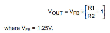
The input bias current of FB has a maximum value of 100nA, which allows large-value resistors to be used. For less than 1% error, the current through R2 should be greater than 100 times the feedback input bias current
(IFB).
For this design, we selected R2 = 75kΩ. The corresponding value of R1 can be calculated as follows:
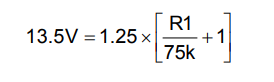 The above expression evaluates R1 = 735kΩ. A standard 732 kΩ value is selected as R1: R1 = 732kΩ.
Step 2: Diode Selection
The high switching frequency of 500kHz requires a highspeed rectifier. Schottky diodes with low forward voltage drop are ideal for this design. A 20V single Schottky rectifier (STMicroelectronics STPS0520Z) with a forward voltage drop of 320mV is selected for this design.
Step 3: Current Limit Selection
The MAX1606 allows a selectable inductor current limit of 125mA, 250mA, or 500mA. This allows flexibility in designing for higher current applications or for smaller, compact designs. The lower current limit allows the use of a physically smaller inductor in space-constrained low-power applications.
The peak current limit required for the application can be calculated from the following equation:
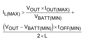
where tOFF(MIN) = 0.8µs and VBATT(MIN) is the minimum voltage used to supply the inductor. The set current limit must be greater than this calculated value. Also, we have to leave some allowance for losses due to diode drop and the parasitics in the board.
For example:
VBATT(MIN) = 1V VOUT = 13.5V
IOUT(MAX) = 10mA
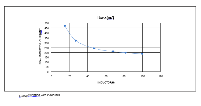 For different values of inductors, the variation of peak inductor current requirement can be seen from Figure 3.
Step 4: Inductor Selection
Smaller inductance values typically offer smaller physical size for a given series resistance or saturation current. On the other hand, circuits using larger inductance values can start up at lower input voltages and exhibit less ripple, but also provide reduced output power. This occurs when the inductance is sufficiently large to prevent the maximum current limit from being reached before the maximum on-time expires. The inductor’s saturation current rating should be greater than the peak switching current.
As discussed before, the parasitics in the board and diode drop play an important role in the amount of power that would be delivered. In our design, the lowest battery voltage for which we need to deliver power to the output is 1V. Using large value inductors can start up the voltage at very low input voltages, however, the amount of power that can be delivered is highly compromised. Therefore, the inductor selection requires a bit of prototyping the circuit to analyze the output behavior with the selected inductor.
For our design, the specifications are as follows:
V BATT(MIN) = 1V
V OUT = 13.5V
I OUT(MAX) = 6mA t OFF(MIN) = 0.8µs
Initially we tested with three inductor values: 10µH, 15µH and 27µH, respectively.
10 µH Testing
To calculate the maximum peak inductor current for this inductor, our design specification in the previous IL(MAX) equation is as follows:
13.5×6m (13.5 −1)×0.8µ
IL(MAX) > +
1 2×10µ
IL(MAX) > 581mA
Selecting a 10µH inductor requires the peak inductor current to be greater than 581m A. Because the device’s maximum inductor current rating is 500mA, the 10µH inductor is not suitable for this design and we have to increase the inductance so that peak current requirement is reduced.
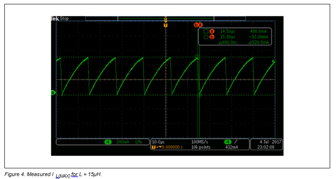
15 µH Testing
Similarly, to calculate the maximum peak inductor current for this inductor, input our design specification again into the previous IL(MAX) expression as follows:
13.5×6m (13.5 −1)×0.8µ
IL(MAX) > +
1 2×15µ
IL(MAX) > 414mA
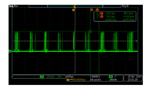
A 15µH inductor requires the peak inductor current to be greater than 414mA, which is well within the device’s current handling capability even after adding some parasitic effects that could increase this requirement on a practical PCB board. The 15µH inductor seems suitable for this design. The prototyped 15µH inductor’s peak inductor current measured is 520mA, as shown in Figure 4, which is showing approximately 20% deviation from the calculated value. The device is successfully delivering 6mA at 1 V battery voltage at an output of 13.5V.
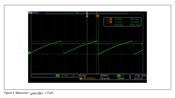
27 µH Testing
We used a 27µH inductor to see the effect of higher inductance on the output power capability. To calculate the maximum peak inductor current for this inductor, we input our design specification again into the previous IL(MAX) equation as follows:
13.5×6m (13.5 −1)×0.8µ
IL(MAX) > +
1 2×27µ
I L(MAX) > 266mA
A 27µH inductor seems suitable for this design as its calculated peak inductor current is well below the maximum allowable value of 500mA. The prototyped 27µH inductor’s peak inductor current measured is 348mA as shown in Figure 5, which is again showing approximately 20% deviation from the calculated value. However, power delivering capability is highly compromised here as high inductance doesn’t allow the current to reach its maximum allowable value before the on time elapses. The output voltage degrades to 12.7V at 6mA. The device is not successfully delivering 6mA at 1V battery voltage at an output of 13.5V.
On the basis of above analysis, we can conclude that 15µH inductor is the most optimum selection, which not only allows the required power delivery to the load, but also allows the circuit to turn on at the required minimum VIN of 1V. The inductor selected for this design is Würth Elektronik’s’ 7447779115. It has an inductance value of 15µH with an ISAT of 2.2A.
Step 5: Output Capacitor Selection
Selecting the correct output capacitor, COUT, and its related ESR is very important for minimizing output voltage ripple. For most applications, use a small 1µF ceramic surface-mount output capacitor. For small ceramic capacitors, the output ripple voltage is dominated by the capacitance value.
Step 6: Output Power vs. VIN (MIN) Trade-Off
The output power supplied is mainly limited by the low input voltage of the battery. As discussed before, the duty cycle is governed by a pair of one-shots that set a minimum off-time and a maximum on-time. The switching frequency can be up to 500kHz and depends upon the load and input voltage. Thus, power delivery to the load at a certain inductor value can be increased by increasing the value of V IN(MIN) available. This should be evaluated by the measurements. Measurements showed that to supply 10mA with our current design, we must increase the available V IN(MIN) value to 1.2V.
Design Resources
Courtesy: www.maximintegrated.com