


Description
This is a backup power reference design for automotive E-Call application. It uses one cell LiFePO4 as the backup battery. The minimum backup battery voltage can be down to 2 V with boost converter TPS61088-Q1. The boost converter TPS61088-Q1 can output 8V/1.6A at 2V input voltage. The value this has over the integrated solution competition is much better efficiency and less redundancy when boosting from the back-up battery.


Features
- Wide input voltage range: 3.8 – 36 V
- 8 V/1.6A output power capability when backup battery voltage drop to 2 V
- Longer Battery Lifetime
- Low cost
- Simple and flexible
Applications
Emergency call (eCall)
Telematics control unit
1 System Description
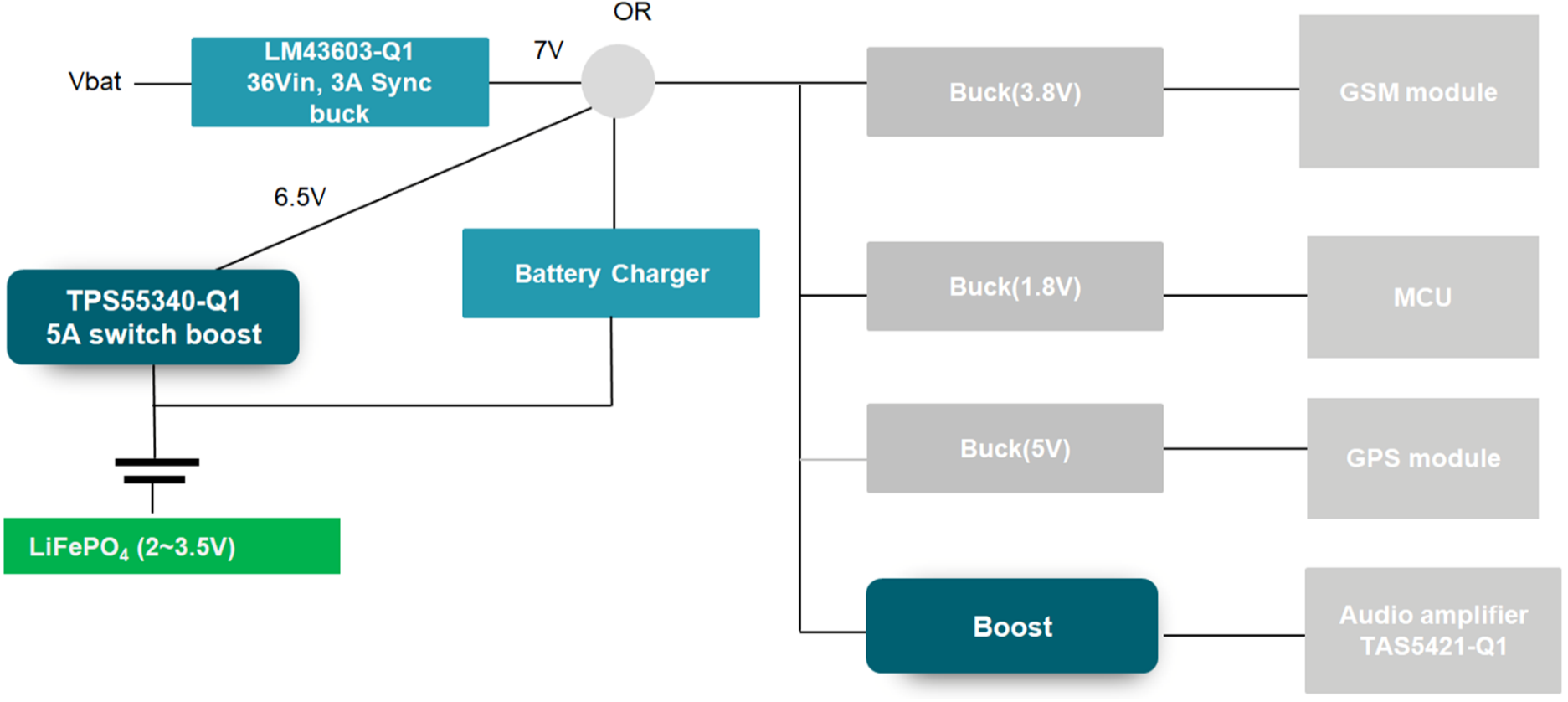
In the E-call application, when the main battery voltage is high, all of the related circuits in the E-call is supplied by the main battery through a buck converter. When the main battery voltage drops to a low level, the buck converter browns out, the back-up battery starts working, it supplies the equipment through a boost converter. Figure 1 shows a traditional E-Call block diagram. Besides a high-voltage buck converter,
Figure 1. Traditional E-call Block Diagram
The TIDA-050031 takes into consideration cost and the size while avoiding the redundancy of a traditional e-Call block diagram in Figure 1. This reference design delivers a simple and low cost backup power circuit for the automotive E-Call application. The structure is very simple. Only one boost converter is used in the circuit. The boost converter TPS61088-Q1 can output 8V/1.6A with high efficiency at 2V input voltage. So the minimum backup battery voltage can be down to 2V. Besides extending the lifetime of the backup battery, the TIDA-050031 is also flexible and less redundancy.
1.1 Key System Specifications
Table 1 provides the TIDA-050031 performance specification. The linear charger charges the back-up battery with a constant 100mA current. The maximum backup power can reach 12.8W when the backup battery drops down to 2 V.
Table 1. Key System Specifications
| KEY FEATURES | DESIGN TARGET | NOTE | |
| Linear Charger Current | 100mA | ± 25% tolerance | |
| Maximum Backup power | 8 V/1.6A | @2 V backup battery voltage |
2 System Overview
2.1 Block Diagram
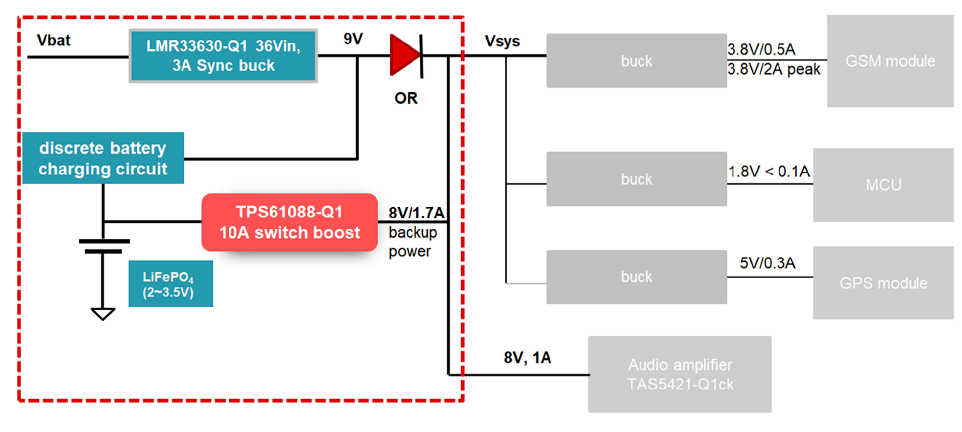
Figure 2 shows the block diagram of TIDA-050031. The output voltage of the buck converter is set at 9 V. The backup battery is charged by this 9 V voltage through the linear charger. After the main battery voltage drops low and the buck converter LMR33630-Q1 browns out, the linear charger stops working. The backup battery supplies the energy for the E-Call system through the boost converter TPS61088-Q1.
Figure 2. TIDA-050031 Block Diagram
2.2 Design Considerations
A key feature of this reference guide is that when the buck converter browns out, the TPS61088-Q1 boost converter can supply voltage to the system immediately. The TPS61088-Q1 boost converter is always enabled to work. When the buck converter works normally and output 9 V, this 9 V voltage added at the output of the TPS61088-Q1, makes the FB pin voltage higher than 1.3V, so the TPS61088-Q1 stops switching, it works at the low power dissipation mode, the current draws from the input side is less than 3 uA.
2.3 Highlighted Products
This reference design adopts the following devices:
- TPS61088-Q1 is a 10-A Fully-Integrated Synchronous Boost Converter
- LMR33630-Q1 is a wide input voltage 3-A Synchronous step-down voltage converter
- TPS7A2501 is a 300-mA, 18-V, Ultra-Low IQ, Low-Dropout Linear Voltage Regulator with Power-Good
- ATL431AIBDZR is a Low Iq Adjustable Precision Shunt Regulator
2.3.1 TPS61088-Q1
The TPS61088-Q1 is a 2.7 V to 12 Vin high power density, synchronous boost converter designed to provide a high efficiency, small size solution for automotive applications. The TPS61088-Q1 has a min input voltage of 2.7 V and therefore can act as a boost for a single or two cell Li-Ion Back-Up Battery (BUB) in applications such as E-Call that also require a high power output to drive the speaker, antenna and other circuits.
2.3.2 LMR33630-Q1
The LMR33630-Q1 automotive-qualified regulator is an easy-to-use, synchronous, step-down DC/DC converter that delivers best-in-class efficiency for rugged applications. The LMR33630-Q1 drives up to 3 A of load current from an input of up to 36 V. The LMR33630-Q1 provides high light load efficiency and output accuracy in a very small solution size. Features such as a power-good flag and precision enable provide both flexible and easy-to-use solutions.
2.3.3 TPS7A2501
The TPS7A2501 low-dropout (LDO) linear voltage regulator introduces a combination of a 2.4-V to 18- V input voltage range with very-low quiescent current (IQ). These features help modern appliances meet increasingly stringent energy requirements, and help extend battery life in portable-power solutions. The TPS7A25 is available in both fixed and adjustable versions. For more flexibility or higher output voltages, the adjustable version uses feedback resistors to set the output voltage from 1.24 V to 17.64 V. Both versions have a 1% output regulation accuracy that provides precision regulation for most microcontroller (MCU) references.
2.3.4 ATL431AIBDZR
The ATL431AIBDZ are three-terminal adjustable shunt regulators, with specified thermal stability over applicable automotive, commercial, and industrial temperature ranges. The output voltage can be set to any value between Vref (approximately 2.5 V) and 36 V, with two external resistors.
2.4 System Design Theory
Figure 3 shows the linear charger circuit of TIDA-050031. The benefits of the linear charger are simplicity and low cost. Transistors Q2 and Q3 are added to limit the initial charge current and makes the charging current a constant value. The existance of Q2 and Q3 can also avoid Q1 being damaged in a short-circuit condition.
Figure 3. Linear Charger Circuit
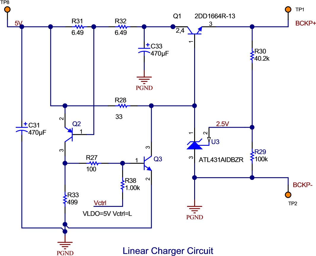
Figure 4 shows the TPS61088-Q1 boost converter of TIDA-050031, which is the main circuit of TIDA050031. The Vin pin of TPS61088-Q1 is supplied by the output voltage through a diode. When the main battery is available, the buck converter is working, Vout is around 8.7V, so the Vin pin voltage is around 8.4V considering the forward voltage drop of D2. The EN pin is pulled high to Vcc. So once the main battery is available and the buck converter starts working, the TPS61088-Q1 is enabled at the same time. In this condition, the operating quiescent current at the Vin pin is less then 3uA, and this quiescent is drawn from the Vout instead of the backup battery. So the backup battery lifetime can be greatly prolonged in this configuration.
Figure 4. TPS61088-Q1 Boost Converter
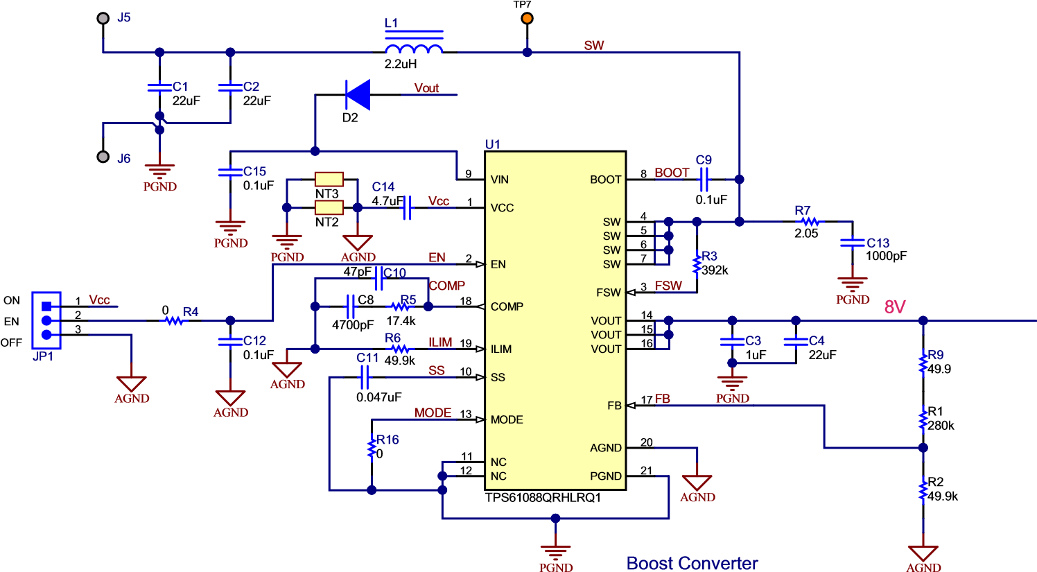
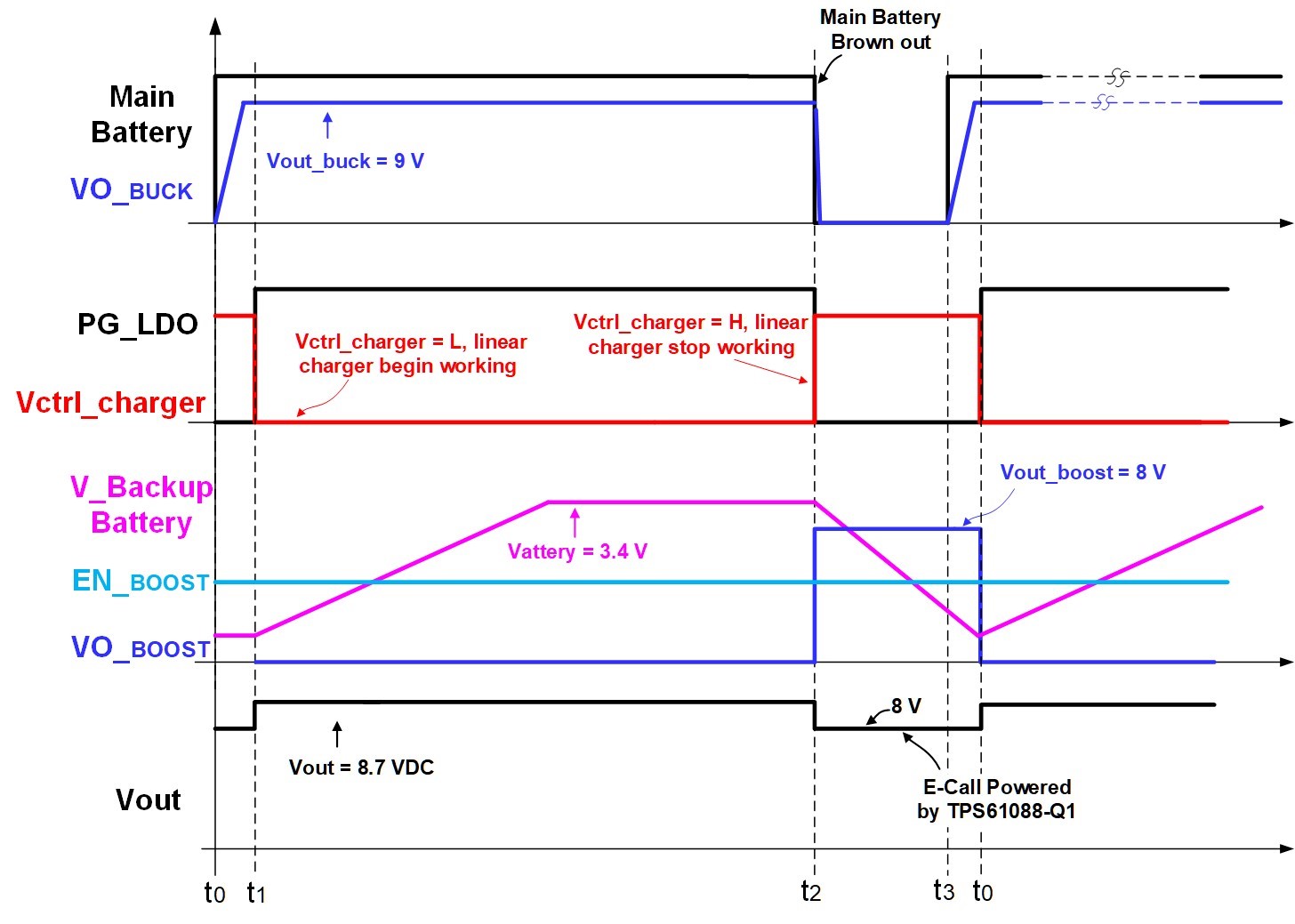
Figure 5 shows the operation sequence of TIDA-050031. At time t0, main battery ready. Buck converter starts working. At time t1, LDO output 5V, the PG pin of the LDO gets high, linear charger begin working, it charges the backup battery with a 100mA constant current. At time t2, the main battery browns out, linear charger stops working, the E-Call system is powered by the backup battery though the TPS61088Q1 boost converter. At time t3, the main battery recovery, it supply the E-call system through the buck converter again.
Figure 5. Operation Sequence
3 Hardware, Software, Testing Requirements, and Test Results
3.1 Required Hardware and Software
3.1.1 Hardware
This reference design uses the following hardware to do the measurement:
- 10A output capability DC power supply
- 2A rating E-load
- Digital oscilloscope
- Signal generator
3.2 Testing and Results
3.2.1 Test Setup
This section describes how to properly connect and set up the TIDA-050031:
- Enable the Buck converter, LDO and the TPS61088-Q1 boost converter;
- Connect the positive terminal of DC power supply to J1(Vin), its GND terminal to J2 ( GND);
- Turn on the DC power supply, set the load current to 1.5 A;
- After one hour, when the backup battery charges up, turn off the DC power supply;
- TPS61088-Q1 starts working;
- Turn off the DC power supply.
3.2.2 Test Results
Figure 6 and Figure 7 show the charge voltage and the charge current across a 2000mAh LiFePO4 capacitor. The initial charge current is well limited. The charge current is 100 mA.
Figure 6. Charge Voltage and Charge Current-1
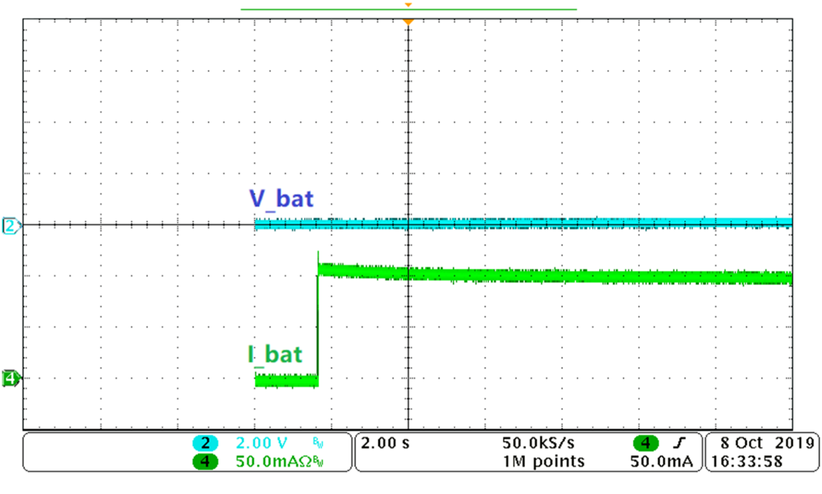
Figure 7. Charge Voltage and Charge Current-2
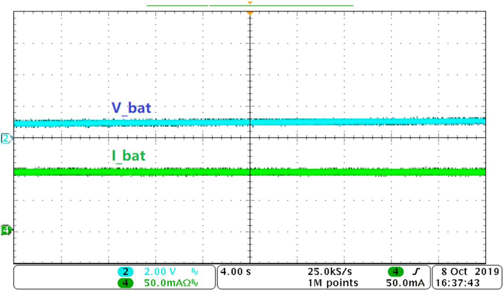
Figure 8 shows the conversion efficiency of the TPS61088-Q1 boost converter under 1.5A load current.
The conversion efficiency is quite high even the backup battery voltage drops to 2 V.
VIN (V) D001
About the Author
Helen Chen has more than 15 years of application experience in power-supply product design. She is familiar with various topologies such as RCC, buck-boost, full-bridge, half-bridge, flyback, CCM PFC, and DCMB PFC. She is also familiar with the magnetic components design, PCB layout, and EMI solutions.