

2D semiconductors could have notable advantages over conventional bulk semiconductors, such as silicon. Most notably, their greater resistance to short-channel effects could make them particularly promising for the development of highly performing transistors, which are crucial components of all electronic devices.
Researchers at Hunan University have recently developed highly performing transistors based on bilayer tungsten diselenide, an inorganic 2D compound with semiconducting properties that were found to perform as well as existing silicon transistors with similar channel lengths and driving voltages.


When evaluating transistors based on 2D semiconductors, engineers can consider different parameters, including their carrier mobility and contact resistance. These two values, however, are mere estimations that can be miscalculated or misinterpreted, resulting in inconsistent estimations of a device’s performance.
The ON-state current density, the amount of electric current flowing through a specific area while a device is operating, has been found to be a far more reliable evaluation parameter. In their study, the researchers thus specifically focused on developing a transistor that had an ON-state current density comparable to that of similar silicon-based devices.
“ON-state current density (Ion) or saturation current density is a more direct and reliable measure of assessing transistors with 2D semiconductors,” Xidong Duan, one of the researchers who carried out the study, told TechXplore. “It remains an open question whether 2D transistors may match, compete or surpass the state-of-art silicon transistors. To answer such question is essential for inspiring more serious interest from the industry community.”
Most 2D transistors developed to date exhibit an Ion value that is significantly inferior to those of silicon devices with comparable channel lengths (Lch) and drain-source bias (Vds). This ultimately limits their potential for real-world, practical applications.
In their previous studies, Duan and his colleagues synthesized ultra-thin 2D metal and in-situ grown 2D metal/semiconductor heterojunctions to build high-quality field-effect transistors. In addition, they created damage-free van der Waals (vdW) electrical contacts that could be used to characterize the intrinsic properties of 2D semiconductors.
“Although 2D metals, such as vdW electrical contacts could improve the performance of 2D semiconductors devices, such excellent electrical properties were achieved with a relatively long channel length, while ultrashort channel devices with vdW electrical contact for evaluating the performance of 2D semiconductors still presented challenges,” Duan said. “The fabrication of ultrashort channel devices often requires aggressive high-resolution lithography and metallization processes, which could introduce undesired contaminations or damages to the atomically thin 2DSCs, and thus seriously compromising their electronic performance.”
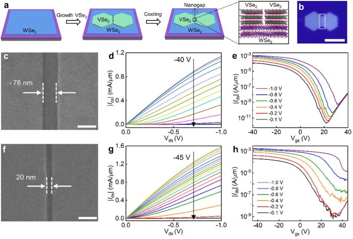
Building on their previous findings, Duan and his colleagues utilized a natural crack formation process to create a gap between merged VSe2 domains grown on bilayer WSe2. This allowed them to develop ultrashort channel bilayer WSe2 transistors with optimized synthetic vdW contacts, achieving a record-high ON-state current density of 1.72 mA/μm and a lowest linear resistance of 0.50 kΩ·μm at room temperature.
“Our results demonstrate for the first time that 2D transistors can deliver competitive current density at a comparable channel length and driving voltage when comparing to the traditional Si transistors,” Duan said. “It gave a positive answer to the long-standing question in the field of “whether 2D transistors can achieve comparable or better performance than the silicon transistors.”
So far, most approaches for fabricating devices with ultrashort channels involved the use of aggressive techniques, including high-resolution lithography and metallization processes. While these techniques can be effective, they also introduce undesired contaminations or damage the anatomically thin 2DSCs, which can seriously compromise the devices’ electronic performance.
When fabricating their transistor, Duan and his colleagues thus decided to take a different approach. More specifically, they used a clean vdW contact and ultrashort channel, which was defined by the thermal stress-controlled nanocrack formation. This allowed them to retain the WSe2 transistor’s original structure and performance as much as possible.
“The obtained ultrashort channels are generally rather straight, distinct from lithographically defined electrodes that often exhibit finite line edge roughness, which creates a good condition for exploring the limit performance of WSe2 transistors,” Duan explained. “In addition, bilayer WSe2 materials typically have smaller bandgaps and better immunity to the fabrication induced damages or interfacial scattering, compared with their monolayer counterpart.”
In initial evaluations, the researchers observed remarkable on-state current densities of 1.0–1.7 mA μm-1 in sub-100 nm bilayer WSe2 transistors, exceeding the critical current density target for 2D transistors (i.e., 1.5 mA μm-1). Their findings could thus have valuable applications for the field of electronics engineering, as they show that transistors based on 2D semiconductors can deliver competitive current densities at channel lengths and driving voltages that are comparable to those of silicon-based transistors.
“We believe the realization of the current density beyond the 1.5 mA/mm has made a positive answer to the long-standing question in the field of ‘whether 2D transistors can achieve comparable or better performance than the silicon transistors,'” Duan said. “It could inspire additional efforts from both the academic and industry community to promote the development of a new generation of 2D semiconductor and chip technology after silicon-based semiconductor.”
In the future, the recent work by Duan and his colleagues could encourage other teams to develop similar devices based on WSe2 or other 2D semiconductors. However, the devices they developed so far are not yet fully optimized. For instance, the team was forced to create them using relatively thick back-gate dielectrics (i.e., 70 nm SiNx), as high-quality dielectrics can be hard to integrate on dangling-bond-free 2D surfaces. The dielectrics used to have a rather small gate capacitance, which can limit the device’s gate coupling efficiency and the extent to which gates can be controlled.
“Our next studies will focus on developing high-quality gate dielectrics with minimum equivalent oxide thickness and minimum interface state to achieve stronger gate control, higher current (closer to the long-term targets of 3.0 mA μm−1), smaller subthreshold swing (closer to the theoretical value 60 mV/dec) and lower Ioff (100 pA μm−1), making the overall key performance parameters of 2D transistors have obvious advantages over silicon transistors,” Duan added. “In addition, we plan to further improve the integration of 2D transistors to promote the commercial application of 2D transistors by combining the large-area growth of 2D semiconductor TMD and 2D metal, advanced lithography process to pattern 2D metal contact arrays, and scalable vdW integration process.”