

, a recently discovered family of two-dimensional (2D) semiconductors could)
Singapore University of Technology and Design (SUTD), a recently discovered family of two-dimensional (2D) semiconductors could pave the way for high-performance and energy-efficient electronics. It may lead to the fabrication of semiconductor devices applicable in mainstream electronics and optoelectronics—and even potentially replace silicon-based device technology altogether.
In the quest of miniaturizing electronic devices, one well-known trend is Moore’s law, which describes how the number of components in the integrated circuits of computers doubles every two years. This trend is possible thanks to the ever-decreasing size of transistors, some of which are so small that millions of them can be crammed onto a chip the size of a fingernail. But as this trend continues, engineers are starting to grapple with the inherent material limitations of silicon-based device technology.


“Due to the quantum tunneling effect, shrinking a silicon-based transistor too small will lead to highly uncontrollable device behaviors,” said SUTD Assistant Professor Ang Yee Sin, who led the study. “People are now looking for new materials beyond the ‘silicon era’, and 2D semiconductors are a promising candidate.”
2D semiconductors are materials that are only a few atoms thick. Because of their nanoscale size, such materials are strong contenders as replacements for silicon in the quest of developing compact electronic devices. However, many currently available 2D semiconductors are plagued by high electrical resistance when they come into contact with metals.
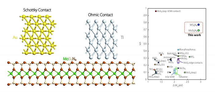
“When you form a contact between metal and semiconductor, often there will be what we call a Schottky barrier,” explained Ang. “In order to force electricity through this barrier, you need to apply a strong voltage, which wastes electricity and generates waste heat.”
This piqued the team’s interest in Ohmic contacts, or metal-semiconductor contacts with no Schottky barrier. In their study, Ang and collaborators from Nanjing University, the National University of Singapore and Zhejiang University showed that a recently discovered family of 2D semiconductors, namely MoSi2N4 and WSi2N4, form Ohmic contacts with the metals titanium, scandium and nickel, which are widely used in the semiconductor device industry.
Furthermore, the researchers also showed that the new materials are free from Fermi level pinning (FLP), a problem that severely limits the application potential of other 2D semiconductors.
“FLP is an adverse effect that happens in many metal-semiconductor contacts, and is caused by defects and complex materials interactions at the contact interface,” Ang said. “Such an effect ‘pins’ the electrical properties of the contact to a narrow range regardless of the metal used in the contact.”
Because of FLP, engineers are unable to tune or adjust the Schottky barrier between the metal and semiconductor—diminishing the design flexibility of a semiconductor device.
To minimize FLP, engineers usually employ strategies like very gently and slowly positioning the metal on top of the 2D semiconductor, creating a buffer layer between the metal and semiconductor or using a 2D metal as a contact material with the 2D semiconductor. While these methods are feasible, they are not yet practical and are incompatible with mass fabrication using mainstream industry techniques available today.
Amazingly, Ang’s team showed that MoSi2N4 and WSi2N4 are naturally protected from FLP due to an inert Si-N outer layer that shields the underlying semiconducting layer from defects and material interactions at the contact interface.
Because of this protection, the Schottky barrier is ‘unpinned’ and can be tuned to match a wide array of application requirements. This improvement in performance helps put 2D semiconductors in the running as replacements for silicon-based technology, with major players like TSMC and Samsung already expressing interest in 2D semiconductor electronics.
Ang hopes that their work will encourage other researchers to probe more members of the newly discovered 2D semiconductor family for interesting properties, even those with applications beyond electronics.
“Some of them might be very poor in terms of electronics applications but very good for spintronics, photocatalysts or as a building block for solar cells,” he concluded. “Our next challenge is to systematically scan through all of these 2D materials and categorize them according to their potential applications.