


– Jacko Wilbrink, Senior Director, Product Marketing, Atmel
– Lionel Perdigon, Product Marketing Manager, Atmel
The ARM Cortex-M series is undisputedly the dominant processor family for embedded systems that require low power and cost effectiveness with moderate performance. The earliest implementations of the Cortex-M processor were on the small end of the spectrum: the Cortex-M0 for lowest cost, the Cortex-M0+ for best energy efficiency, the Cortex-M3 for best power/performance balance, and the Cortex-M4 for applications requiring digital signal processing (DSP) capabilities.
Now the first implementations of the highest-performance member – the Cortex-M7 – are emerging. This processor includes capabilities required for more complex algorithms running at higher speeds while still maintaining modest energy consumption and cost profiles. In a 65nm embedded Flash process device, the Cortex-M7 can achieve a 1500 CoreMark score while running at 300 MHz, and its DSP performance is double that available in the Cortex-M4. A double-precision floating-point unit and a double-issue instruction pipeline further position the Cortex-M7 for speed.
Thanks to these features, the Cortex-M7 becomes a natural choice when serious algorithms for audio and video are needed for rich audio and visual capabilities in low-power, low-cost applications. The Cortex-M7 has found a home in the image processing of drones, and the audio, voice control, object recognition, and complex sensor fusion of automotive and higher-end Internet of Things (IoT) sensing.


Tightly coupled Memories for Fast, Deterministic Code Execution
It is often the case that such algorithms as FIR, FFT or Biquad need to run as quickly and deterministically as possible for real-time response or seamless audio and video performance. To meet system performance and latency goals, such routines should operate at the full clock rate, unencumbered by cache misses, interrupts, context swaps, and other execution surprises that work against deterministic timing.
This means that you cannot simply run such code out of standard memory, and you cannot rely on standard memory for storing the data being processed. Typical memories like Flash are too slow to keep up with the Cortex-M7 core, and they require caching, causing long delays when a cache miss occurs. So the Cortex-M7 architecture provides a way to bypass the standard execution mechanism using “tightly coupled memories,” or TCM.
The ARM core provides the TCM interface, and it is intended for single-cycle random TCM access running at the full processor speed. A 64-bit instruction memory port (ITCM) supports the dual-issue processor architecture, and two data ports (DTCM) enable two simultaneous, parallel 32-bit data accesses. The architecture does not, however, specify what type of memory or how much memory should be provided. Those decisions are left to designers implementing the Cortex-M7 core in a microcontroller (MCU) as opportunities for innovation and differentiation.
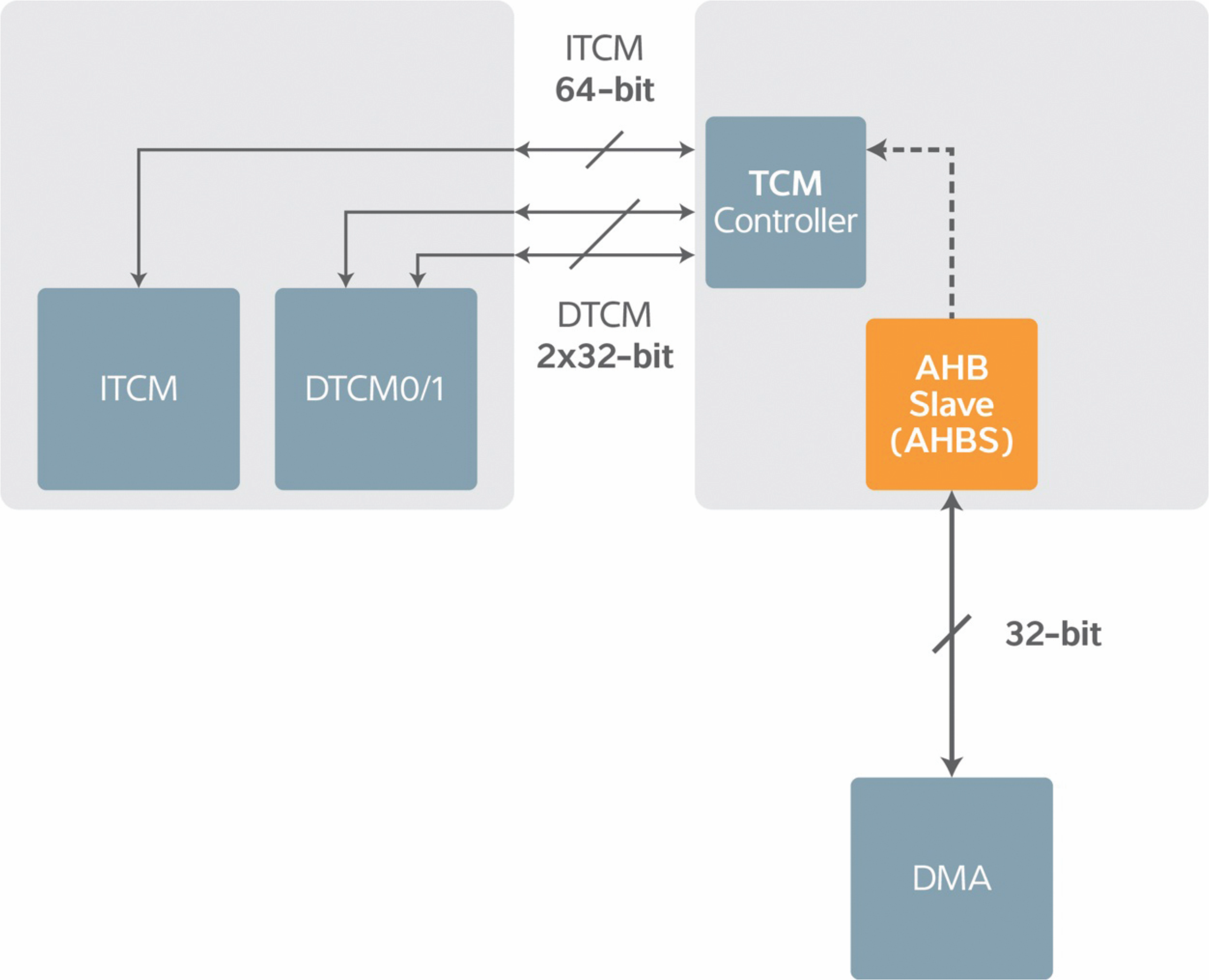
So, for instance, it is possible to attach embedded Flash memory to the TCM interface. But Flash cannot run at the processor clock rate, so caching would be required – threatening the determinism that the TCM is intended to provide. Code shadowing in DRAM is theoretically possible, but it would be cost-prohibitive. The only type of memory that is fast enough for direct, uncached access is SRAM. SRAMs provide a number of benefits: an SRAM block can be connected directly to the TCM interface, SRAM technology is easily embedded on-chip, and SRAMs permit random accesses at the speed of the processor. The only drawback of SRAM is the cost per bit, which is higher than that of Flash and DRAM. So it is critical to keep the size of the TCM limited, even if 65- or 40-nanometer technology allows a fair amount of SRAM integration at acceptable cost. The TCM might be loaded from a number of sources, and these are also not specified by the architecture. So MCU implementations may vary in how these memories can be loaded. A direct-memory access (DMA) engine would certainly be involved, but whether it is a single DMA or one of several loading data from various streams like video or USB is left to the MCU designer.
The code that will be executed out of the TCM is identified by the system programmer. When preparing a software build, the programmer will need to identify which code segments and data blocks should be allocated to the TCM. This is typically done by embedding pragmas into the software and by applying linker settings so that the build places code and memory appropriately.
Multiple Ports for Faster SRAM Access
While TCM provides a straightforward mechanism for quick, tight execution of key routines, it is often useful to have some amount of system SRAM as a general-purpose, high-speed memory for the processor and peripherals to use by means of a DMA. While such memory would logically be separate from the TCM, it is possible that a single SRAM block could share TCM and general-purpose duties while offering the possibility to tune the split between TCM and system RAM for each use case.
Peripheral data buffers implemented in general-purpose system SRAM are typically loaded by DMA transfers from system peripherals. The ability to load from a number of possible sources, however, raises the possibility of unnecessary delays and conflicts by multiple DMAs trying to access the memory at the same time.
In a typical example, we might have three different entities vying for DMA access to the SRAM: the processor (64-bit access, requesting 128 bits for this example) and two separate peripheral DMA requests (DMA0 and DMA1, 32-bit access each). Let us assume that the processor has priority over the DMAs and that DMA0 has priority over DMA1.
This example is illustrated in Figure 2. The left shows the performance of a 64-bit wide single-banked memory; the right shows the same transactions in the same memory organized as four 32-bit banks.
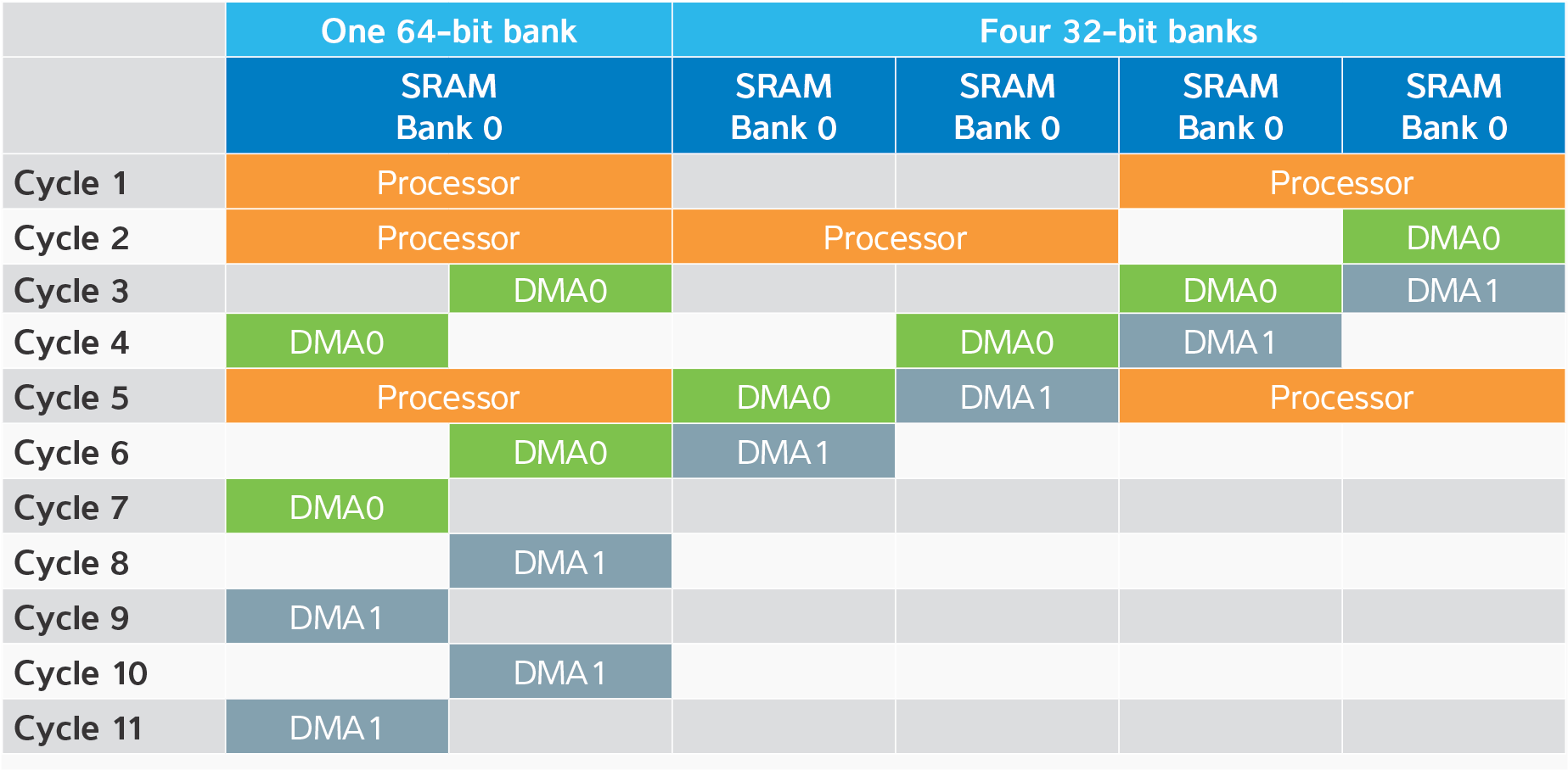
With the single-bank memory, the processor would complete its access in two cycles, and then, in the next cycle, the DMA0 burst would start. DMA1 would be blocked until DMA0 was finished. Any higher-priority processor requests would interrupt the DMA loads, adding further delays. As shown above, an instruction fetch in Cycle 5 adds another cycle of delay to both DMA operations.
More efficient operation can be achieved by organizing the memory into banks with interleaved addresses, each of which can be independently accessed. In this manner, the DMA0 burst would begin when the processor was done with the first bank – simultaneous to the processor accessing the higher banks. DMA1 would no longer have to wait until the entire DMA0 transfer was complete; it could start one cycle after DMA0, when DMA0 was finished with the first bank.
Having higher priority, the processor sees no latency difference between the two arrangements. But DMA0’s latency improves from two cycles to one, and DMA1’s latency goes from seven cycles down to two. An instruction fetch during the DMA operations may even occur in parallel with the DMA operations, resulting in no additional latency. Lower latency improves performance, but it may also mean that you can make peripheral FIFOs smaller.
Given these possible useful memory arrangements, it is left to the MCU designer to figure out how Flash memory, system SRAM, and TCM work together. Are they all separate? Do they occupy similar space? On- or off-chip? These decisions will differentiate competing Cortex-M7 implementations.
A Specific Cortex- M7 TCM Example
One example of a Cortex-M7 MCU is implemented in the Atmel | SMART SAM S70, SAM E70, and SAM V70/1 families. These MCUs have an SRAM organized into four banks that can be used as general SRAM (which Atmel calls System SRAM) and for TCM. In the portion configured as TCM, instructions can run with deterministic, single-cycle access at the full core speed of 300 MHz, with no delays for fetches or caching. Similarly, data located in TCM can be accessed without caching penalties. The Instruction TCM (ITCM) and data TCM (DTCM), which must be sized alike, can be 32, 64, or 128 KB each. This sizing is a build-time setting that cannot be changed on the fly.
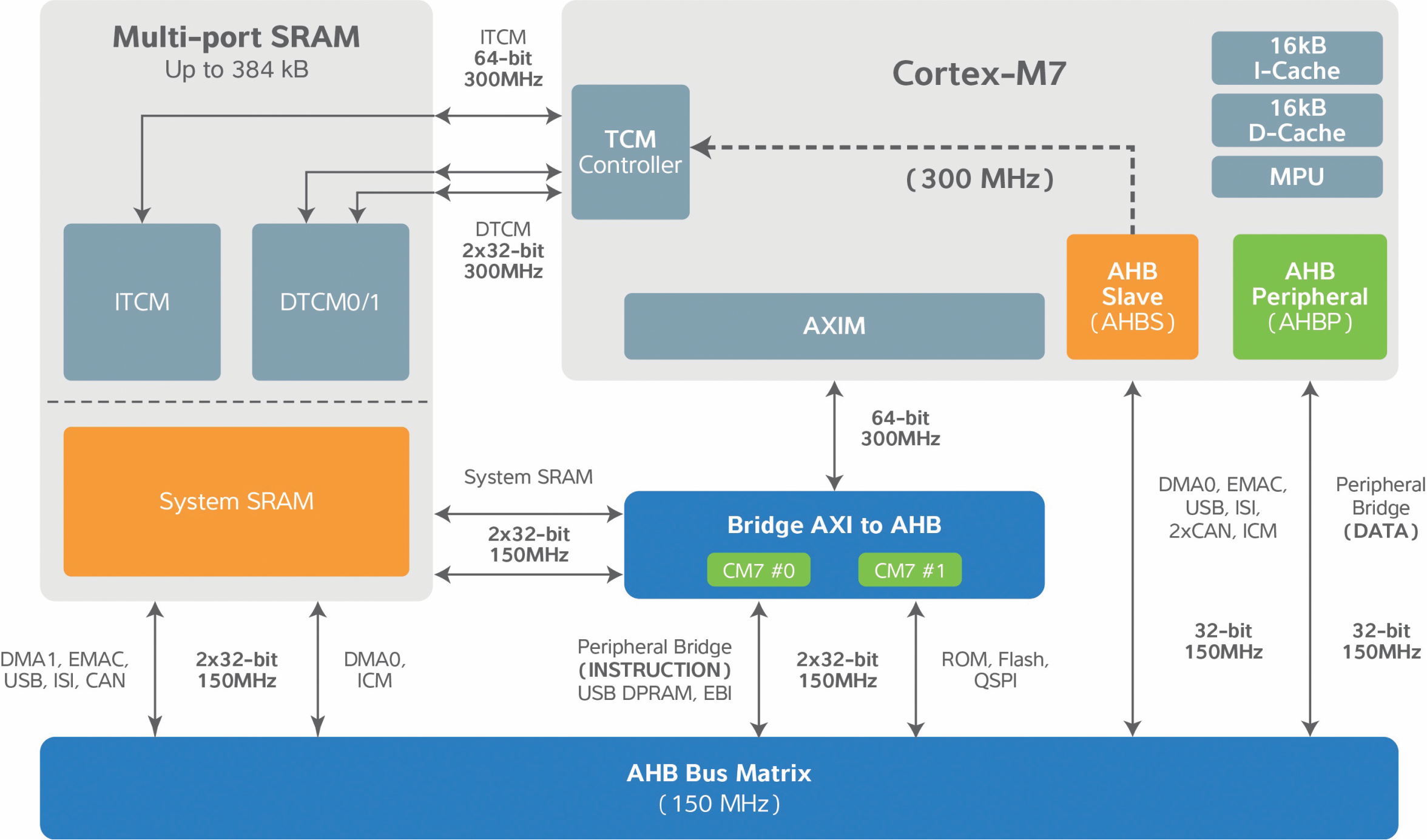
The full SRAM block can be up to 384 KB in size. That means that both System SRAM and TCM can be used at the same time. The amount of memory configured as TCM reduces the amount of memory available for use as System RAM; for example, if configured for 128 KB of ITCM and 128 KB of DTCM, then the amount of System RAM is reduced to 128 KB. The System SRAM runs up to 150 MHz, or half the processor speed, and it is organized into four banks, reducing DMA latency. DMA access priorities, which can be fixed or round robin, are the same for system SRAM as they are for the internal bus matrix. A register bit activates or deactivates the TCM, so the target of a given access will depend on TCM activation. A device is always booted with ITCM deactivated, allowing code to be loaded from the boot memory. After booting, the TCM can be activated as needed.
The ITCM address space overlaps the boot memory. If TCM is deactivated, then instruction accesses go to the boot memory. If TCM is activated, then accesses within the TCM address space come from the TCM; accesses above the TCM space come out of Flash. It is possible to protect the various spaces with the MPU to ensure that there are no inadvertent accesses to the wrong memory.
Cortex-M7 Is the Next ARM Wave
 The Cortex-M7 is coming into its own, taking on much more aggressive algorithms while still remaining gentle with power and cost. Tightly coupled memories, one of the new Cortex-M7 features, make possible the fast execution of tight code with deterministic execution at the full processor clock rate. Exactly how this performance will be realized on a given MCU will depend on system choices made by the designers integrating the Cortex-M7 into the MCU. The highest speeds will be afforded by using SRAM to implement the TCM. This SRAM can be shared with a more general system SRAM capability, and, by organizing the SRAM in banks, DMA latency can be minimized. These architectural features, while relatively simple, provide a dramatic boost to the performance available for implementing critical embedded functions in personal, industrial, and automotive devices.
*The white paper can be downloaded from the atmel webpage-http://www.atmel.com/technologies/cpu_core/arm/cortex-m7.aspx