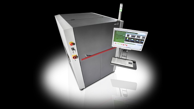
Despite the major improvements that have been made, the Solder Paste Inspection on modern circuits is far more complicated than boards were even a few years ago. The introduction of surface mount technology and the subsequent further reductions in size mean that boards are particularly compact. Even relatively average boards have thousands of soldered joints, and these are where the majority of problems are found. Solder paste inspection inspects the solder paste printed PCB for defects like less or excess solder, missing solder, solder shift, solder short and solder volume. SPI uses two types of techniques to analyse whether a board is satisfactory or has any defects.
Laser measurement system: Two laser beams are projected from opposite directions to eliminate the risk of shadowing. The beams are then scanned onto the PCB and reflected back to a high-resolution camera (CMOS) to calculate height with X-Y spatial resolution. The result is a highly accurate 3D model construction.
Camera measurement system: Angled cameras are used to take 3D images, which help to measure the alignment and volume of the solder paste. SPI systems compare the image with the program.
Solder Paste Inspection systems can be placed into the production line just after the solder printing process. In this way they can be used to catch problems early in the production process. This has a number of advantages. With faults costing more to fix the further along the production process they are found, this is obviously the optimum place to find faults. Additionally, process problems in the solder and assembly area can be seen early in the production process and information used to feedback quickly to earlier stages. In this way a rapid response can ensure that problems are recognized quickly and rectified before too many boards are built with the same problem.
Solder Paste Inspection is mainly done to check the solder paste deposits in the Printed Circuit Board (PCB) manufacturing process. It is observed that most of the solder joint defects in a PCB assembly are because of improper solder paste printing. With the help of solder paste inspection (SPI), you can reduce the defects related to soldering by a considerable amount. This post will explain the significance of SPI process and how it is essential.
Importance of Solder Paste Inspection Process
Here are some of the key points of information, which prove the importance of SPI process:
- Improves PCB Quality & Performance:This process makes use of advanced equipment for precise inspection. Angle cameras are used to take 3D pictures, which are very helpful in measuring the alignment and volume of the solder paste. This helps improve the yield, as well as the print quality. Furthermore, it helps improve the performance of the PCBs.
- Advanced Equipment for Better Control & Monitoring:As said earlier, angle cameras are used, which produce clear 3D pictures. Unlike the traditional cameras, 3D cameras are capable of capturing the height of the solder paste printed. This facilitates precise measurement of the solder paste volume. Thus, with the help of SPI coupled with automated optical inspection, manufacturers can easily monitor and control the component placement and solder paste printing processes.
- Helps Reduce Solder Error: Important information about the printing process can be obtained by doing the solder paste inspection. It gives a clear idea about the causes of defects, thus allowing you to make the necessary changes and reduce the errors to a minimum.
3D solder paste inspection has the ability to not only check for solder paste area coverage and shorts but can also accurately measure the shape and volume of the solder paste deposits. The key aspects when considering 3D solder paste inspection are as follows:
Inspection speed: Most machines will have a specified inspection speed measured in cm2/sec – ensure machine selected is capable of keeping up with the process time of the largest board to be processed. The image below shows an example PCB relative to the field of view (FOV) of the inspection machine.
Programming training: It is important to have data that exactly represents the stencil being used and so the expected solder paste deposits. Solder paste information within data is usually a 1:1 copy of the pads of the track layer. This information will be sent to the stencil manufacturer who will go through a process of modifying the data according to a predefined specification such as size reductions.
Accuracy: This system works well but one of the factors that can limit the repeat-ability is the number of projectors installed within the machine. Using a single projector can lead to shadows depending on the height of the solder paste deposits which can lead to inaccurate measurements being taken. The solution to this problem is to increase the number of projectors which will improve repeat-ability and accuracy but will also increase the cost of the machine.
Yield Improvement: Use of 3D SPI significantly shortens any new product or process introduction as the data being displayed is based on measurements being taken and not image interpretation. When processing large batch numbers another feature to consider is the ability to connect SPI machine to the printer to enable automatic adjustment of certain parameters such as the alignment.
There are many manufacturers in the market using different technologies and so it is important to consider the points above before choosing a particular machine. It’s also important to consider the needs of the company as some options will be more important than others and some may not be necessary.
As assemblies become more complex and components used become smaller it will become more difficult to control the solder paste printing process without automating the inspection process. Solder paste inspection machines are a significant investment but the benefits of tightly controlling the manufacturing process will pay back in the long term by reducing rework and improving yield. Now Let us also have a look at some of the SPI systems launched:
Koh Young KY8030-3
The latest SPI system from Koh Young Technologies Inc. offers accurate and fast 3D measurement capabilities that address the shortcomings and vulnerabilities of conventional paste inspection systems and 2D SPI/AOI systems.
CyberOptics Corporation SE3000
The new SE3000 SPI system has incorporated the industry-leading MRS sensor technology with a finer resolution for accuracy, repeatability and reproducibility —even on the smallest paste deposits. Combined with easy-to-use SPI software, the SE3000 has the capability to work on large boards.
Omron VP6000-V
The VP 6000-V has a unique 3D process for measuring the volume of solder used in screen printing. It guarantees reliability and repeatability of high quality. The choice of resolution for the purpose, as well as the setting of standards, is done by software
Pemtron TROI 7700 series
Using Moire’s pattern, Pemtron’s three-dimensional lead application dosage tester combines 2D colour images with 3D measurement data to provide more detailed, near-real PCB images, unlike traditional colour maps.
Given the importance of controlling the solder paste printing process and the effect on the complete process if a defect is not detected early, the investment in a 3D solder paste inspection machine should be seriously considered.
There are many manufacturers in the market using different technologies and so it is important to consider the points above before choosing a particular machine. It’s also important to consider the needs of the company as some options will be more important than others and some may not be necessary.
As assemblies become more complex and components used become smaller it will become more difficult to control the solder paste printing process without automating the inspection process. Solder paste inspection machines are a significant investment but the benefits of tightly controlling the manufacturing process will pay back in the long term by reducing rework and improving yield.
It’s a shocking statistic to read that within the electronics industry many surface mount operations, particularly within the sub-contract manufacturing sector, run as low as 20% efficient.
There are many reasons that contribute to this figure but it fundamentally means that only 20% of the capital investment is being utilized. Financially, this will lead to a higher cost of ownership and a slower return on investment. For the customer, it can cause longer lead times for their product and therefore the business will not be as competitive in the market place.
At the end of 2019, COVID-19 began to erupt in China, Due to the huge decrease of global economy, it has shown a decrease. This is percentage points lower than in previous years. With the slowdown in world economic growth, the 3D Solder Paste Inspection (SPI) System industry has also suffered a certain impact, but still maintained a relatively optimistic growth, the past four years, 3D Solder Paste Inspection (SPI) System market size to maintain the average annual growth from 2015 to 2020, BisReport analysts believe that in the next few years, 3D Solder Paste Inspection (SPI) System market size will be further expanded by 2025. With production efficiency at this level there will be many knock-on effects that will have an impact on the business such as larger batch sizes, more parts in stock, more assemblies in WIP (work in progress) and slower reaction times to customer change requirements.


