Introduction
Electronic warfare (EW) receivers must intercept and identify unknown enemy signals among a congested wideband spectrum of multiple interfering signals without the benefit of dynamic range and sensitivity improvement techniques employed in communications and radar receivers. The incident RF band limiting employed in communications receivers is an unwanted trade for the EW receiver that seeks to process ever wider instantaneous bandwidth in less time. In the radar realm, receiver dynamic range benefits from matched filtering, whereby the received radar return is correlated with a copy of the transmitted signal. Alas, the EW receiver has no prior knowledge of the signal to be intercepted and thus nothing with which to correlate! It’s like searching a crowd of people for a stranger you’ve never seen before … and worse yet, he is hiding, or maybe isn’t even there!


Now for the good news: over the coming years, high sample rate analog-to-digital converter (ADC) and digital-to-analog converter (DAC) technology will usher in a wideband digital receiver architectural evolution. Most importantly, converters from Analog Devices will maintain the excellent linearity, noise performance, and dynamic range of legacy lower rate digital converters. The workhorse super-heterodyne tuner will give ground to direct sample and direct conversion architectures. Adaptive spectral tuning will continue to shift from the RF to the digital signal processing realm.
This sea change in wideband RF sensing will enable size, weight, power, and cost (SWaP-C) benefits: higher receive and transmit channel counts at lower cost per channel, in the same or smaller sized form factors as today.
Anticipating the coming era of digital EW receivers with multi-octave bandwidth, this article discusses new challenges and considerations when designing for best-in-class dynamic range. In this article, dynamic range refers to instantaneous spur free dynamic range, the key figure of merit for receivers tasked with detecting small signals among a crowded spectrum of larger blockers.
Next-Generation ADC Performance
Many of today’s EW receivers feature sub-octave instantaneous bandwidth (IBW) that is limited by the older generation data converter. These will be replaced tomorrow with multi-octave wideband digital receivers spanning several GHz of IBW. For example, in the coming years a growing number of sensing platforms will employ ADI converter chips featuring ADCs and DACs with the ability to process greater than 4 GHz IBW while maintaining SFDR greater than 70 dB.
A popular low SWaP, wideband digital receiver ADC use case might be:
- An ADC sample rate of ~15 GSPS
- A direct sample of the first Nyquist zone (that is, dc to 6 GHz)
- A direct sample of the second Nyquist zone (that is, 8 GHz to 14 GHz)
- RF block convert middle (6 GHz to 8 GHz) and higher (>14 GHz) bands
EW receivers need to cover higher and higher swaths of spectrum from 18 GHz to 50 GHz and beyond. The ADC’s high second Nyquist zone eases the frequency plan, allowing simple RF front-end block converters with relaxed, smaller SWaP RF filters. The following discussion considers an RF front end cascaded with a high sample rate ADC similar to the previous example.
Dynamic Range in Wideband Digital Receivers
Receiver designers optimizing dynamic range must balance sensitivity (NF) with linearity (IP2, IP3) as these RF device attributes usually move against each other. Dynamic range is bound by sensitivity at lower RF levels and linearity at higher RF levels. As a rule of thumb, the maximum allowed receiver operating level is set so that the multisignal intermodulation distortion (IMD) spurious levels are equal to the noise power, as shown in Figure 1. Modern systems use adaptive instantaneous bandwidth channelization and processing bandwidths (Bv), which moves the noise floor up and down 10Log(Bv). The nuanced topic of processing bandwidth is critical and receives its own discussion later.
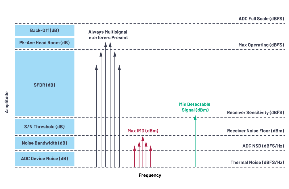
Figure 1. Relating SFDR to ADC operating range, noise, IMD spurs, and detection threshold.
Multi-Octave IMD2 Challenges in Wideband Digital Receivers
The wideband digital receiver evolution introduces new RF challenges. Multisignal second-order intermodulation distortion (IMD2) spurs emerge as problematic dynamic range impairments in the multi-octave wideband digital receiver. While IIP3 has long been a key figure of merit (FOM) in RF device data sheets, IIP2 is harder to track down and can be more problematic to the EW designer. The problem with IMD2 spurs is that they only fall off by 1 dBc for every 1 dB decrease in the incident 2-tone signal power, while third-order intermodulation distortion (IMD3) spurs fall off by 2 dBc.
Of course, multi-octave direct RF sampling at the lower portion of the ADC first Nyquist zone is nothing new. For example, an older system might sample at 500 MSPS and observe dc to 200 MHz in the first Nyquist zone with no IMD2 problems. This is because at these lower frequencies (that is, less than a few hundred MSPS), ADC characteristics are highly linear and the effective IIP2 and IIP3 of the ADC is very high, resulting in benign IMD2 products invisible below the noise floor. Just like in wideband RF devices, however, multi-GHz, multi-octave ADC linearity will degrade with increasing frequency, and IMD2 products will often sit above the noise floor at higher operating frequencies. Going forward, we’ll need to deal with IMD2.
Broadened SFDR Definition for Wideband Digital Receivers
IMD2 crashing the party requires a refreshed definition of the popular receiver FOM instantaneous spurious-free dynamic range (SFDR). SFDR specifies how far down a receiver can detect a small signal when there are multiple larger signals creating IMD spurs. SFDR is specified in dB relative to the large signals.
Traditionally, SFDR is defined in terms of IMD3 products, along with NF and processing bandwidth. IMD3-referenced SFDR is derived in many texts, and is sometimes clarified as instantaneous SFDR, which is what we mean in this article. We’ll call it SFDR3:
Today IMD2-referenced SFDR receives less attention, but it is looming on the horizon as a major impairment needing mitigation. It can be derived in the same manner as SFDR3. Here we’ll call it SFDR2:
![]()
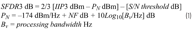
Figure 2 illustrates an RF front-end spectral scenario whereby three simultaneous signals (F1, F2, and F3) create intermodulation products that set the lower bound to dynamic range. Below this level, the wideband digital receiver can’t easily tell whether a target is real or a false IMD spur.
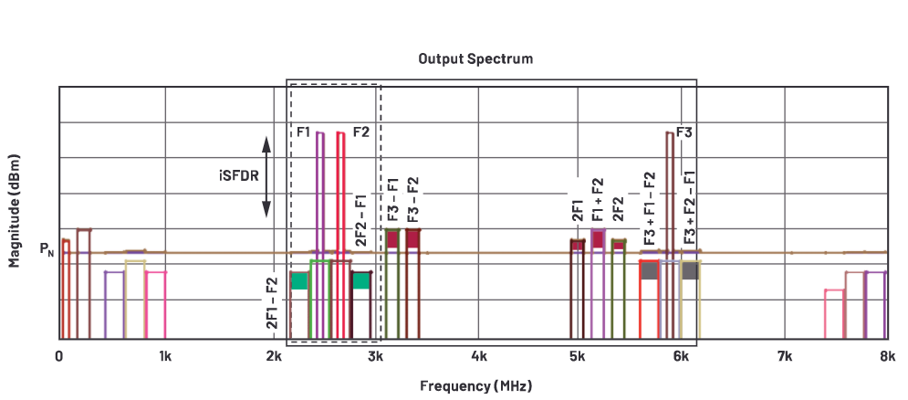
Figure 2. An example of multisignal F1, F2, and F3 (60 MHz each) inducing second-harmonic, IMD2 (red), IMD3 (green), and IMD2/3 combo (gray) spurs. The noise floor (brown) is noted as PN.
The sub-octave IBW receiver of today, notionally shown by the Figure 2 dashed box, worries only about IMD3 because it falls in-band and cannot be filtered. It doesn’t worry much about IP2 because of the easily filtered location of IMD2 and the inducing signals. F3 is easily chopped down using input RF filtering, which takes F3 – F1 and F3 – F2 way below the noise floor. Much like the F1 and F2 second harmonics, the F1 + F2 IMD2 is easily attenuated using output filtering. Of course, the second-order performance of the ADC must be considered in relation to Nyquist folding spurs, but the front-end IMD2 performance is easy to deal with.
Enter the multi-octave IBW receiver, notionally shown by the Figure 2 solid box, and the situation turns on its head. IMD2 is the bigger concern vs. IMD3. The IMD2 spurs and inducing interferers are now in-band. Band-pass filtering them defeats the purpose of a multi-octave IBW. This is why tunable notch filtering, despite its limitations, is seeing increased attention as a front-end interference mitigator. It doesn’t lop off giant pieces of the multi-octave spectrum.
Figure 3 illustrates the relationship between the fundamental multi-tone large signal, IMD2 and IMD3 level, noise floor, and the resulting SFDR for an example multi-octave wideband digital receiver. The example uses real noise and linearity attributes for an ADC sampling the first Nyquist zone with a 4 GHz IBW from 2 GHz to 6 GHz. A processing bandwidth of 469 kHz is assumed.
Figure 3. SFDR2 and SFDR3 tell you how far down from the largest signal (fundamental) you can easily detect a smaller signal. Because it varies widely, the detection threshold is zero here. In practice, subtract your detection threshold from SFDR.
Optimal SFDR2 and SFDR3 occur at different Pin operating points where the respective IMD level intersects the noise power. If we pretend for a moment that this is a sub-octave receiver with front-end RF band-limiting, SFDR3 sets the overall SFDR, and we can expect a best case SFDR of 79 dB, which is very good. But since the EW receiver requires multi-octave IBW, SFDR2 sets the overall SFDR. At the best SFDR3 input level (Pin = –20 dBm), the IMD2 spurs degrade the SFDR by 24 dB, resulting in an SFDR of 55 dB. Fair, albeit disappointing, results.
A useful rule of thumb is that for a specific RF output level = PRF,O to achieve equivalent IMD2 and IMD3 levels:
![]()
In other words, this condition will make the SFDR2 and SFDR3 lines intersect the noise floor at the same spot, so that SFDR2 is not limiting performance.
For the previous SFDR example scenario, the RF front end feeds the ADC with –20 dBm and has an OIP3 of 20 dBm. The required OIP2 to get the same level IMD2 and IMD3 spurs, and thereby not limit performance, is:
![]()
That raw device OIP2 performance is not available today given the balance with other attributes like frequency, bandwidth, noise, and dc power. This explains the increasing interest in next-generation adaptive front-end interferer mitigation techniques.
To mitigate IMD2, the receiver must lower the max input operating level from –20 dBm to –32 dBm, and is then able to achieve an improved SFDR2 of 66 dB best case. In Figure 3, this optimal SFDR2 is where the IMD2 trace intersects the noise floor. Alas, the best case SFDR2 at Pin = –32 dBm is still 13 dB worse than the best case SFDR3 at –20 dBm. Since we’ve now shifted the max operating level down, this puts the spotlight on noise power (sensitivity) limitations, as discussed in the next sections.
What Sets Processing Bandwidth in the Wideband Digital Receiver?
The sensitivity, or noise power, of the EW receiver gets better as the processing bandwidth narrows. In typical fashion, however, there are trade-offs to balance: we can’t just reduce the bandwidth to an arbitrarily small value and head to lunch. What are the competing factors to consider? To answer the question, we need to discuss decimation, the fast Fourier transform (FFT), and their relationship. First, we define a couple variables:
ADI’s high sample rate ADCs employ on-chip digital signal processor (DSP) blocks that allow configurable filtering and decimation of the raw data stream to a minimum viable payload sent to the downstream FPGA. This process is discussed in detail across ADI literature. The obvious benefit of decimation is reducing the digital payload that must pass over JESD204B/JESD204C to the FPGA. Another benefit is the power consumption savings realized using local on-chip decimation-specific circuitry (that is, ASIC) vs. implementing the same operation in the FPGA fabric. But local on-chip decimation is beneficial beyond just thinning the data stream and saving power. We’ll get to that.
Figure 4 shows the blocks used in modern wideband digital conversion (as relevant to this discussion). The flow consists of sampling, digital downconverting, digital filtering, decimating, and fast Fourier transforming the data stream.
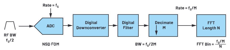
Figure 4. Simple block diagram of ADC data decimation and FFT.
First, the data sampled at fS is digital downconverted to baseband (complex I/Q) using a fine-tuned NCO. The data stream is then filtered using a programmable low-pass digital filter. This predecimation digital filtering sets the IF bandwidth and is the first of two different operations to set the receiver noise floor PN. As the IF bandwidth gets smaller, the integrated in-band noise power decreases as the filtering attenuates the wideband noise.
![]()
Next, decimating by M reduces the effective sampling rate to fs/M, keeping every Mth sample and throwing out the samples in between.
Thus, the downstream FFT processing gets a data stream with rate fS/M and bandwidth fS/2M. Finally, the FFT length N sets the bin width and capture time, which is the second step in setting the noise floor.
![]()
Decimation and FFT Impact to Wideband Digital Receiver Noise Floor
Figure 5 relates the wideband digital receiver’s processing noise floor (K) to the ADC’s noise spectral density (L), which is the widely available data sheet FOM for ADC additive noise. Existing ADI literature does a nice job explaining processing gain, NSD, SNR, and quantization noise.
The most useful relation from Figure 5 is:
The processing noise floor (Figure 5, K) is the same as PN and can be dropped into Equation 1 and Equation 2. Note that the designer carefully selects M and N based upon design trade-offs and constraints discussed in the next section.
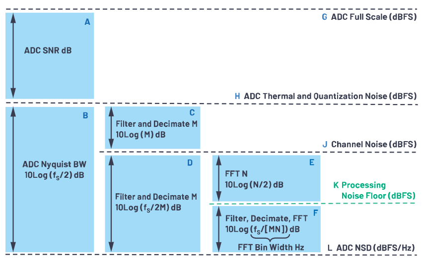
Figure 5. Relationship of decimation and FFT gain operations to commonly referenced noise levels.
Even though increasing the decimation factor M has the same proportional effect in reducing the noise floor (Figure 5, C) as increasing the FFT length N (Figure 5, E), it is important to note the mechanisms are entirely different. The decimation step involves band-limiting the channel using digital filtering. This sets the effective noise bandwidth that determines the total integrated noise in the channel (Figure 5, D). It also sets the maximum instantaneous spectral bandwidth of a detectable signal. Compare this to the FFT step, which does not filter per se, but spreads the total integrated noise in the channel over N/2 bins and defines the spectral line resolution. The higher N, the more bins, and the lower the noise content per bin.8 Together, decimation gain M and FFT gain N define the FFT bin width, and they are often lumped together in discussions of processing bandwidth (Figure 5, F), but their values must be balanced based upon their respective nuanced impact to signal bandwidth, spectral resolution, sensitivity, and latency requirements, as discussed in the next section.
Processing Bandwidth and System Performance Trade-Offs
Relating decimation M and FFT N back to high priority performance attributes:
Latency is the time to sense and process successive spectral captures, and it requires as short a time as possible. Many systems require near real-time operation. This dictates M × N be as small as possible. As the FFT size increases, the spectral resolution improves and noise floor decreases as the integrated noise is spread over more bins. The trade-off is acquisition time, which is a big deal and is simply:
![]()
The minimum detectable pulse width (PW) sets the minimum allowable IF channel bandwidth as the spectral content of a shorter time pulse spreads over a relatively wider frequency band. If the IF channel bandwidth is too narrow, the signal spectral content truncates, and the short time pulse isn’t detected properly. Minimum IF BW, which sets maximum allowable M, must meet the criteria:
![]()
Spectral resolution and sensitivity improve as the FFT bin narrows, which requires increasing N. Longer pulse widths and PRIs require finer resolution to resolve closer spectral lines, which means larger N for proper detection. Increasing N improves spectral line resolution, but only within the IF bandwidth defined by M. If too high a decimation is used, increasing N improves the spectral resolution within the IF BW set by M, but cannot recover the missing signal bandwidth. For example, a pulse train with a pulse width below the minimum receiver pulse width will have a frequency domain sinc function whose main lobe exceeds the decimation bandwidth. Increasing N will help resolve the PRF of the train, but will do nothing to resolve the pulse width; that information is lost. The only fix is to decrease decimation M, increasing the IF bandwidth.
Decimation, FFT, and Detection of Pulse Trains
EW wideband digital receivers spend a lot of their effort de-interleaving, identifying, and tracking simultaneous incident radar pulse trains. Carrier frequency, pulse width, and pulse repetition interval (PRI) are radar signatures that are critical in figuring out who’s who. Both the time and frequency domain are used in detection schemes.9 An overarching objective is to sense, process, and react to the pulse trains in as short a time duration as possible. Dynamic range is critical because the EW receiver needs to simultaneously track multiple distant targets while being bombarded with high energy jamming pulses.
Pulse Train FFT Examples
Two pulse train examples are presented. The first represents a pulsed doppler radar exhibiting a very short PW (100 ns) at 10% duty cycle, resulting in very high PRF. The second simulates a pulsed radar exhibiting comparatively longer PW and PRI (lower duty cycle, lower PRF). The following plots and tables illustrate the impact of decimation M and FFT length N on time, sensitivity (noise floor), and spectral resolution. Table 1 summarizes the parameters for easy comparison. The fictional values do not represent specific radars but are nevertheless in a realistic ballpark.
| Table 1. Comparison of Example Pulsed Doppler and Pulsed Radar Attributes | ||||
| Parameter | Pulsed Doppler Radar | Pulsed Radar | ||
| PW | Short | 100 ns | Longer | 10 μs |
| PRI | Short | 1 μs | Longer | 1 ms |
| PRF | High | 1 MHz | Low | 1 kHz |
| Duty Cycle | Mid/high | 10% | Mid/low | 1% |
| Decimation M | Low | 256 | High | 1536 |
| FFT Length N | Low | 128 to 512 | High | 16,384 to 65,536 |
| Time | Quick | 2 μs to 9 μs | Longer | 2 ms to 7 ms |
| Sensitivity | Lower | –91 dBFS | Higher | –120 dBFS |
The point here is that M and N are not one size fits all, and sophisticated detection algorithms and parallel channelization schemes in any given EW receiver may employ a wide range of values for each. The EW receiver must be able to detect both signals, likely at the same time (not shown here), which is why fast, adaptable configurability is important. Dynamic range and sensitivity are directly dependent on the pulse attributes that must be detected.
Example: Wideband Digital Receiver Sensing Pulsed Doppler Radar
The following two FFTs capture a pulsed doppler scenario.
The first FFT shown in Figure 6 needs just over 2 pulse cycles to determine the pulse width of the signal from the width of the FFT main lobe. The decimation M is set for an IF bandwidth that is adequately wide to capture the main lobe, as well as some sidelobes. The response time is very fast. The trade-off to quick response time is a worse noise floor and spectral resolution. Note that due to the lack of spectral resolution, no PRI information is available in the FFT.
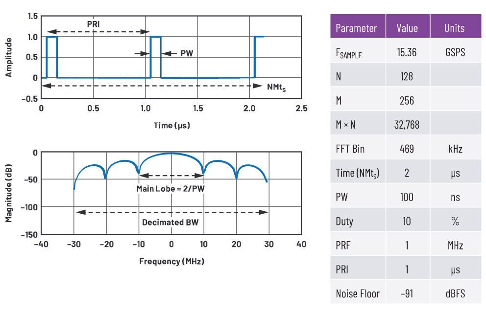
Figure 6. Fast capture of narrow pulse width, high PRF pulse train typical of pulsed doppler radar.
The second FFT in Figure 7 shows an improved noise floor and spectral resolution as sample length N (and time) are increased. M remains the same. By around nine pulse cycles, the spectral resolution improves enough to determine the PRI (1/PRF) from the FFT. The noise floor can be seen between sidelobes.
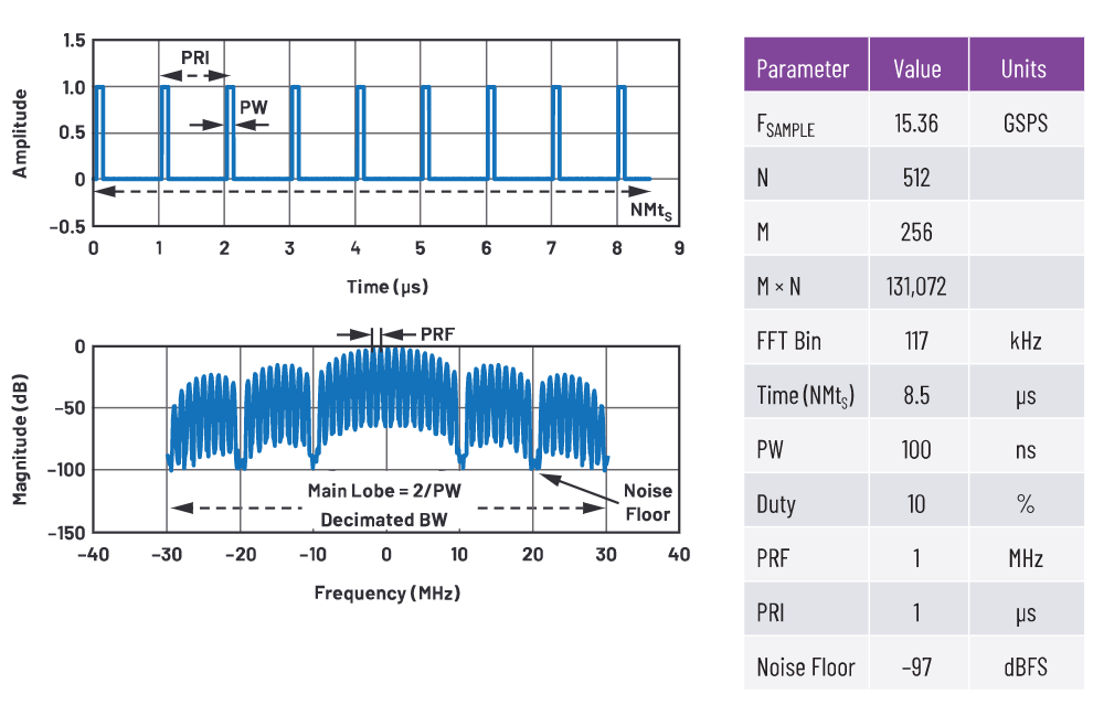
Figure 7. A longer FFT of a pulsed Doppler example to resolve spectral lines.
Example: Wideband Digital Receiver Sensing Pulsed Radar
The following two FFTs capture a wider pulsed scenario.
The much wider PRI, or lower pulse density, in the pulsed radar example in Figure 8 requires much higher N. Adjusting M is entirely system dependent. If the short pulse must be detected simultaneously with the long pulse in the same IF channel, then M must be set to accommodate the short pulse spectral bandwidth and cannot be increased. Considered on its own, the long pulse requires a lower IF bandwidth, so M could be set higher to improve the channel noise and resulting sensitivity. The capture time, or FFT length N, required is a lot longer, however. So it’s likely the detection algorithm would want to make intermediate decisions on the short pulse scenario while the system acquires a high enough N to resolve the long pulse.
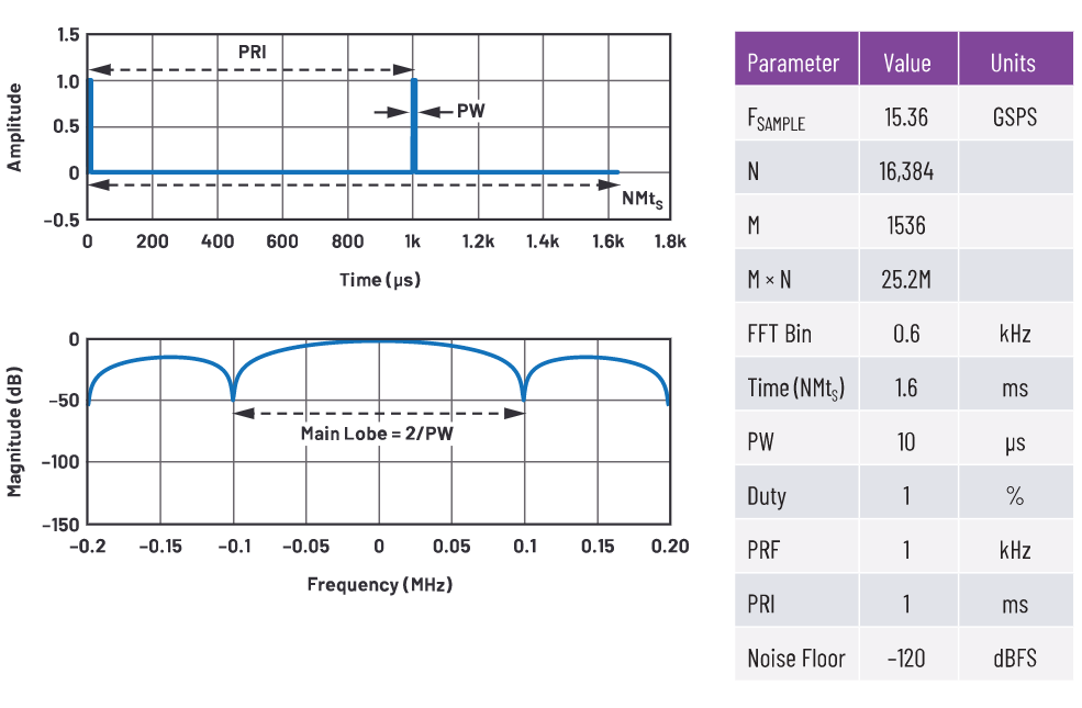
Figure 8. Fast capture of longer pulse, lower PRF pulse train typical of pulsed radar.
The second long pulse FFT example in Figure 9 illustrates how the long PRI (low PRF) results in very close spectral lines, which requires very low FFT bin size or resolution bandwidth. The trade-off is even more time required (FFT N). A benefit is even better sensitivity.
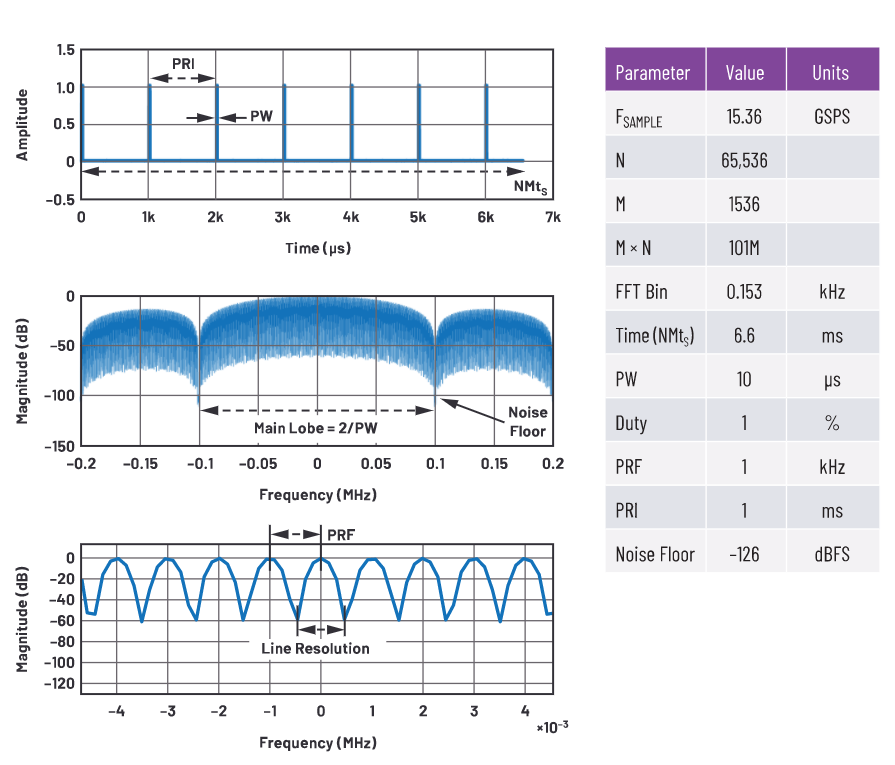
Figure 9. A longer FFT of pulsed example to resolve spectral lines.
Wideband Digital Receiver RF Front-End Design Using a Cascaded ADC
With dynamic range and sensitivity goals established, an RF front end must be paired with the digital data converter. The optimal RF front end sets the receiver sensitivity (NF) and performs the required spectral signal conditioning with good enough linearity head room to allow the ADC performance to set receiver IP3 and IP2. Front-end RF gain is typically set to be good enough to establish the required cascaded NF, as gain beyond that generally hurts dynamic range and is avoided. It is criminal if the front end bottlenecks dynamic range and ADC capability is thrown out!
A helpful trick is to convert the ADC figures of merit to equivalent RF cascade parameters and treat the ADC like an RF black box. Some rules of thumb:
Where PRF (dBm) is the ADC input RF level at which the IMD3 and IMD2 levels are measured.
Note that the cascaded system NF of the combination front end and ADC is broadband noise prior to adjusting for processing gain.
Design Example of Front End to ADC Cascade
An example cascade analysis follows using the front end shown in Figure 10. This chain benefits from the latest ADI releases to the RF catalog, including:
- ADMV8818wideband programmable high-pass/low-pass tunable filter.
- ADRF5730wideband RF SOI digital attenuator.
- ADRF5020wideband RF SOI SPDT.
- ADL8104ultrahigh IP2 wideband RF amplifier.
- AD9082MxFE 4× DAC (12 GSPS) + 2× ADC (6 GSPS)
Additionally, the chain features a wideband 200 W RF limiter and small form factor high Q fixed filtering developed at ADI.
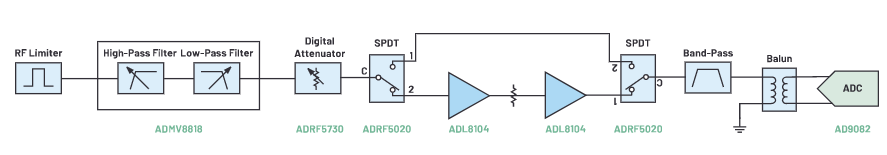
Figure 10. Example RF front end featuring switched high sensitivity and bypass modes.
An age-old technique to preserve dynamic range is to switch between a high sense mode for lower input signals and bypass mode for higher input signals. As shown in Table 2, the high sense path favors NF performance, and the bypass path concedes higher NF in favor of higher linearity (IP2 and IP3). The performance tables illustrate this benefit.
| Table 2. Example RF Front-End Black Box Parameters for the Two Modes | |||||
| Mode | G (dB) | NF (dB) | IIP2 (dBm) | IIP3 (dBm) | IP1dB (dBm) |
| High Sense | 10 | 15 | 31 | 17 | 5 |
| Bypass | –14 | 14 | 75 | 40 | 25 |
Table 3 compares the front end and ADC black box parameters, and the resulting overall cascade performance.
In the high sense mode, the limiting factor to dynamic range is the noise floor, and so cascaded NF is prioritized. The front-end noise figure depends mostly on the insertion loss of the front-end filtering required for interferer mitigation (this example budgets 6 dB loss). This preselect filtering needs to sit before the amplifier to be effective, as the amplifier will create multisignal IMD products.
In bypass mode, we benefit from the extremely high linearity of the SOI technology. No tricks here as the amplifier limited linearity is simply switched out in favor of higher linearity, lower gain, and higher NF.
| Table 3. Example High Sense (top) and Bypass (bottom) Cascaded Performance; the Overall Column Is the Cascaded RF Front End plus ADC All-In Performance | ||||
| RF Front End | ADC | Overall | Units | |
| Full Scale | –6.5 | dBm | ||
| NSD | –148 | dBFS/Hz | ||
| –154.5 | dBFS/Hz | |||
| Gain | 10 | 0 | dB | |
| NF | 15 | 19.5 | 16.1 | dB |
| IIP2 | 31 | 35 | 21.5 | dBm |
| IIP3 | 17 | 20 | 9.2 | dBm |
| Pi | –40 | –30 | dBm | |
| PN | –91.2 | dBm | ||
| RF Front End | ADC | Overall | Units | |
| Full Scale | –6.5 | dBm | ||
| NSD | –148 | dBFS/Hz | ||
| –154.5 | dBFS/Hz | |||
| Gain | –14 | 0 | dB | |
| NF | 14 | 19.5 | 33.5 | dB |
| IIP2 | 75 | 35 | 48.6 | dBm |
| IIP3 | 40 | 20 | 33.0 | dBm |
| Pi | –15 | –29 | dBm | |
| PN | –97.8 | dBm |
Wideband Digital Receiver Design Results and Optimization
The following performance heat maps are sensitivity analyses showing instantaneous spur free dynamic range (DR, dB) for varying:
- Processing bandwidth and RF input level
- RF front-end IIP2 and RF input level
- RF front-end NF and RF input level
Each scenario is run for the high sensitivity and bypass paths. The boxes annotate favorable operating zones. The tables tell you the dynamic range (SFDR), or distance down to the noise floor or highest IMD spur, for a given max input signal level at Pin. For any given table, the static variables are set per the previous chain parameters.
As discussed in prior sections, the Bv selected in Figure 11 is dependent upon waveform detection objectives. Lower Bv decreases the noise floor, improving dynamic range at low Pin, but at the expense of slower FFT times. Inversely, high Bv values increase the noise floor, and poor sensitivity limits dynamic range. The likely operating zone is at a balance point in between.
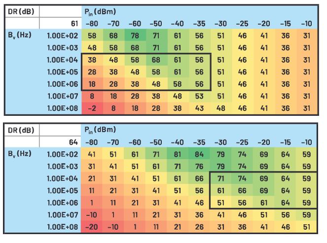
Figure 11. Instantaneous spur free dynamic range (DR) vs. RF input level (Pin) and processing bandwidth (Bv); high sensitivity (top) and bypass mode (bottom).
Figure 12 illustrates that, at low Pin levels, IIP2 is irrelevant as the sensitivity sets the dynamic range. The mid-range performance is most sensitive to IIP2. Mid-range input power levels might comprise most use cases, and as Pin increases toward the high sense to bypass switch point, amplifier linearity, especially IP2, is critically important. The superior IP2 of ADL8104 stands out over this important mid-range, preserving high dynamic range performance.
The bypass mode higher IIP2 allows the operating zone box to shift down to follow the best dynamic range.
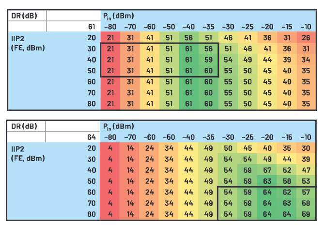
Figure 12. Instantaneous spur free dynamic range (DR) vs. RF input level (Pin) and RF front-end input referenced IP2; high sensitivity (top) and bypass mode (bottom).
Figure 13 shows that for big improvements to NF, which can be very costly to SWaP-C and linearity, there is a diminishing return to dynamic range using a mid-range Bv. For lower NF to pay off, Bv needs to decrease with it and the associated trade-offs tolerated. The high sense mode does well with an NF in the 10 dB to 15 dB range. For the bypass mode, the high NF is shown to be a willing trade-off given the benefit to linearity. Ideally NF can be kept in the 20 dB to 25 dB range for the bypass mode. Better NF in bypass mode doesn’t help dynamic range, as we are IMD limited.
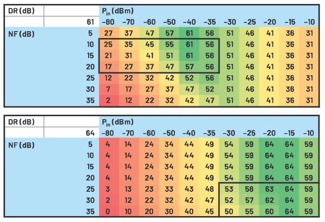
Figure 13. Instantaneous spur free dynamic range (DR) vs. RF input level (Pin) and RF front-end noise figure (NF); high sensitivity (top) and bypass mode (right).
Summary
Electronic warfare’s imminent evolution toward multi-octave, multi-GHz instantaneous bandwidth RF tuners and wideband digital receivers introduce IMD2 effects that challenge dynamic range. Today’s consideration of SFDR in terms of IMD3 will broaden to include IMD2, and the designer will use both the SFDR2 and SFDR3 equations. The system noise floor is dynamic because processing bandwidth changes on-the-fly based upon waveform detection and time requirements. When designing the optimal noise floor, decimation M and FFT depth N together define the FFT bin width, yet they each have separate important impacts to consider. Example pulse train FFTs of varying M and N are provided. As ADC performance improves, the front end continues to rely on high linearity wideband RF components with tunable attributes and frequency selectivity. The front end should be designed in cascade with the ADC’s RF attributes.