


As the semiconductor industry moves to next-generation 3D architectures, the need intensifies for process control solutions that can reduce the time to ramp a technology to production-level yields. Gate-All-Around (GAA) transistors, EUV lithography, and scaled memory devices all present challenging requirements for detection of defects buried within 3D structures. As critical dimensions shrink, these defects can approach single-digit nanometers in size, or only a few atoms thick.
Chipmakers use two tools to find and control manufacturing defects: optical inspection to detect potential defects on the wafer, followed by eBeam review to characterize these defects in more precise detail. Optical inspection and eBeam review are complementary – together they deliver an actionable pareto that engineers can use to optimize yield and ensure faster time-to-market.


A key challenge facing eBeam defect review at the most advanced nodes is the ability to differentiate the true defects from the false alarms presented from the optical inspection systems, while maintaining the high throughput necessary for volume production.
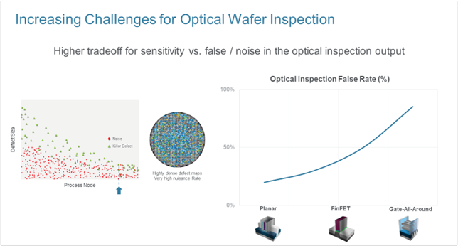
The eBeam review process has become much more challenging as transistors have moved from planar to FinFET and now GAA. The “false rate” – when optical inspection flags something that is not a true defect – more than doubles with the GAA structures. Defects are smaller and killer defects are more difficult to distinguish from noise with GAA and advanced memories. The defect maps created after optical inspection become denser, with a large amount of nuisance (>90%), in order to capture the required defects of interest (DOIs). With such a high nuisance rate, it becomes nearly impossible to deliver an actionable pareto with enough DOIs to achieve statistically significant process control. To compensate for the high number of candidates in inspection, process control engineers need defect review systems that can deliver far more samples than today’s typical benchmark of several hundreds of DOI candidates.
Deep Learning for Defect Classification
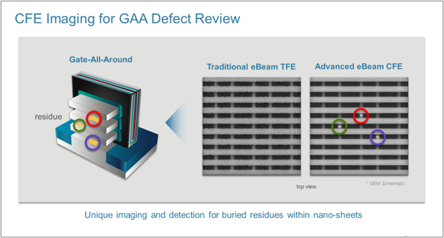
Applied Materials is the leading provider of eBeam defect review systems. In 2022, we introduced our “cold field emission” (CFE) technology, a breakthrough in eBeam imaging that enables chipmakers to better detect and image nanometer-scale, buried defects. We are now extending this technology to address the increased sampling requirements of the high false alarm rates (“High FAR”) of advanced logic and memory.
When combined with the use of back-scattered electrons that enable high-resolution imaging of deep structures, CFE technology allows better throughput while maintaining high sensitivity and resolution compared with previous-generation thermal field emission (TFE) sources – enabling sub-nanometer resolution for detecting the smallest buried defects.
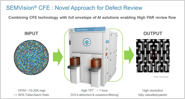
Applied is now combining the use of CFE with deep learning AI technology for automatic extraction of true DOIs from the false “nuisance” defects. In many cases, the actual DOIs are only 5 percent or less of the review candidates. The deep learning network is continuously trained with data from the fab and sorts the defects into a defect distribution including voids, residues, scratches, particles and dozens of other defect types. Defect extraction is highly accurate, with nearly 100-percent accuracy.
3D Devices Need 3D Process Control
The use of Applied-developed AI to enable automatic DOI extraction and classification is a new application. In one use case, the eBeam system considered roughly 10,000 defect candidates of a GAA device. While traditional defect review might be able to sample this many candidates, the new CFE with AI defect review system delivers much greater sensitivity and higher throughput, handling 10,000 candidates in less than an hour. Moreover, the AI-enabled in-line detection, filtering and classification system can classify 4X as many DOIs into specific types. Combining CFE technology with a full envelope of AI solutions makes it possible to deal with the high false alarm rates for 3D structures presented by the wafer inspection systems. CFE offers the required sensitivity to image the challenging defects, at higher throughputs compared with traditional TFE systems. Subsequently, with the help of AI, the required DOIs are captured with high accuracy, filtering out nuisances.
As 3D devices are being deployed in production, Applied has developed defect review technology that can sample 10,000 – 20,000 locations per hour, handle false-alarm rates exceeding 90 percent, and classify the defect types presented to statistical process control solutions. This innovative defect review approach is being successfully demonstrated at leading logic and memory chipmakers. Based on the feedback so far, we see a strong pull from customers as they address the High FAR challenge.

Senior Product Marketing Manager
Applied Materials