US researchers have created an EMI screening material that is semi-transparent flexible and quickly applied, although only to small objects.
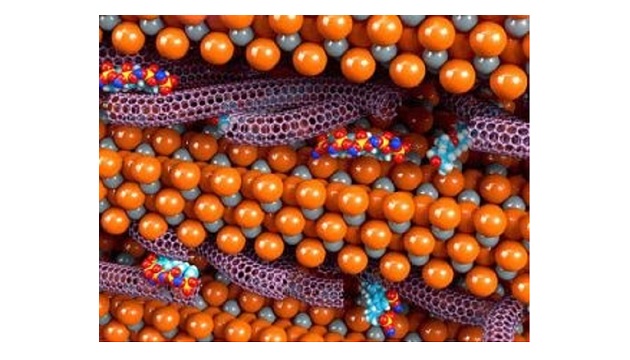
They are films with hundreds of layers, each a few nanometres thick, the polymer-bonded layers alternate between carbon-nanotubes and a MXene. MXenes are two dimensional inorganic molecules containing a transition metal carbide or carbonitrides, in this case titanium carbide MXene.
Their physical characteristics mean that the alternating layers bond strongly together, and both types of layer, particularly the MXene, are electrically conductive.
By altering the number of layers and other details, sheet resistance can be varied over 817Ω/sq to 109Ω/sq, while optical transmittance (at 550nm) increases from ~47% to 91.9%, according to the paper ‘Layer-by-layer assembly of cross-functional semi-transparent MXene-carbon nanotubes composite films for next-generation electromagnetic interference shielding‘, published in Advanced Functional Materials, which goes on to say: “Our MXene-CNT films are highly conductive, environmentally stable, lightweight, flexible, freestanding, and semi-transparent. We suspect even further improvements can be achieved by tuning the ratio of the conductive and the polymer fillers, coupling different polymer fillers and optimising the preparation conditions.”
New York University has lead development of the film, supported by Drexel University, Yale University and Southwest Jiaotong University in China. The deposition technique that can deposit hundreds of layers quickly is ‘spin-spray layer-by-layer processing’ (SSLbL), pioneered by NYU chemical engineer André Taylor.
SSLbL uses spray heads mounted above a spin coater “that deposit sequential nanometer-thick monolayers of oppositely charged compounds on a component, producing high quality films in much less time than by traditional methods, such as dip coating”, said NYU.
“Our system can create hundreds of bi-layers of alternating MXene and CNT in minutes,” said Taylor. “As we worked to discern the roles different components play. We found that the strong electrostatic and hydrogen bonding between oppositely charged CNT and MXene layers conferred high strength and flexibility.” He added that MXene, as well as conducting electrically, has the benefit of easily adhering to a surface.
Because SSLbL allows nm-level control over film structure, conductivity and transparency can be traded predictably, argues NYU, contrasting this with films made by depositing pre-mixed ingredients, for example nanoparticles, polyelectrolytes and graphene.
What SSLbL does not do, is work over large areas. According to Taylor, in theory the system could create EMI shielding for devices and components up to 300mm, the diameter semiconductor wafer, on which spin-coating is frequently employed during processing.


