

Metal halide perovskites are a large class of crystalline materials with numerous advantageous features, including a high light absorption coefficient, high charge mobility and strong photoluminescence. Due to their unique properties, metal halide perovskites have proved to be highly promising for the fabrication of solar cells.
While engineers have so far primarily used these materials to create solar cells or other solar technologies, they can also substitute silicon or other semiconductors in devices that can sense light and other types of radiation, known as photodetectors. Photodetectors are central components of many sensors, imaging tools, optical communication technologies and devices for monitoring the environment.


Researchers at the Dutch Organization for Applied Scientific Research and Eindhoven University of Technology in the Netherlands have recently used a solution-processed photodetector made of a metal halide perovskite to fabricate a thin and flexible scanner. This scanner can be used to scan both fingerprints and paper documents.
“Fabricating photodetectors with low dark currents and integrating them into high-resolution backplanes remains challenging,” Albert J. J. M. van Breemen and his colleagues wrote in their paper. “Here, we show that solution-processed metal halide perovskite photodiodes on top of an amorphous indium gallium zinc oxide transistor backplane can be used to create a flexible image sensor that is ~100 μm thick and has a resolution of 508 pixels per inch.”
Van Breemen and his colleagues fabricated their photodetector using a solution-processed layer of Cs0.18FA0.82Pb(I0.82Br0.18)3, containing caesium (Cs+) and formamidinium (CH(NH2)2 +, FA) cations. Initially, the device was designed to be integrated in solar cells, yet they subsequently decided to test its potential in a scanner.
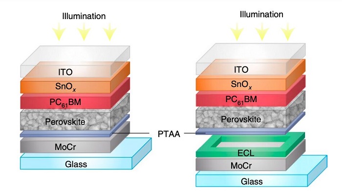
The photodetector followed a so-called inverted stack design, with a molybdenum-chrome alloy (MoCr) as the bottom electrode, coated with a thin HTL layer of PTAA. A [6,6]-phenyl C61 butyric acid methyl ester (PC61BM)–SnOx layer was placed on top of the perovskite active film, acting as an electron transport layer (ETL).
In addition, the team introduced a 50-nm-thick silicon nitride (SiN) edge cover layer (ECL) between the MoCr bottom electrode and the PTAA, which reduced electrode current leakage and consequently dark current density. Finally, they placed a 100-nm-thick transparent indium tin oxide (ITO) electrode on top of the stack and a transparent thin-film encapsulation barrier.
By integrating their photodetector with a thin-film transistor array, van Breemen and his colleagues then created an “all in one scanner.” This scanner can be used to collect high quality images of both fingerprints and documents, with a resolution of 508PPI.
Highly sensitive scanners such as the one created by this team of researchers could have many valuable applications. Most notably, they could help to prevent spoofing attacks on biometric sensors. During spoofing attacks, attackers can gain access to sensitive user information on their personal devices, impersonating them using synthesized copies of their biometric data.
By capturing high-resolution images of fingerprints and other important documents, the scanner created by van Breemen and his colleagues could be used to identify fake documents or synthesized fingerprints with greater accuracy and precision. In addition, this recent study could pave the way towards the integration of perovskite image sensors or photodetectors in smartphones or other commonly used devices, to strengthen the efficiency of biometric identification tools.