

 are high-performance and cost-effective electroluminescence devices that are ideal for)
Planar perovskite light-emitting diodes (LEDs) are high-performance and cost-effective electroluminescence devices that are ideal for large-area display and lighting applications. By exploring the emission layers with high ratios of horizontal transition dipole moments (TDMs), researchers can boost the photon outcoupling of planar LEDs. The LEDs that are based on anisotropic perovskite are inefficient due to the challenges of regulating the orientations of TDMs as well as the difficulties of achieving high photoluminescence quantum yields, including challenges of realizing charge balance in the films of assembled nanostructures. In this work, Jieyuan Cui and a research team in chemistry, materials science and optics in China, showed efficient electroluminescence emanating from an in-situ perovskite film made of a monolayer of nanoplatelets. The team achieved LEDs with a peak external quantum efficiency (EQE) of 23.6 percent to represent highly efficient planar perovskite LEDs.
The photon emission characteristics in semiconductors are based on transition dipole moments. Molecules in a material can attain an excited or non-excited state through the absorption and emission of light, where the rules of transition dipole moment and quantum mechanics can help predict if the transition to an excited state is likely. Nanoplatelets and nanorods that comprise optical transition dipole moments within materials are highly anisotropic and their structure-property relationship is of interest for planar light-emitting diodes (LEDs). Generally, transition dipole moments are horizontally oriented for light coupling and those that are vertically oriented contribute to energy loss. Metal halide perovskites are another emerging class of solution-processed semiconductors with interesting properties including high photoluminescence quantum yields and tunable emission wavelengths. In this report, Cui et al. described efficient LEDs based on in situ grown perovskite films to show high ratios of horizontal transition dipole moments and high photoluminescence quantum yields.


Structural characterization of nanoplatelets
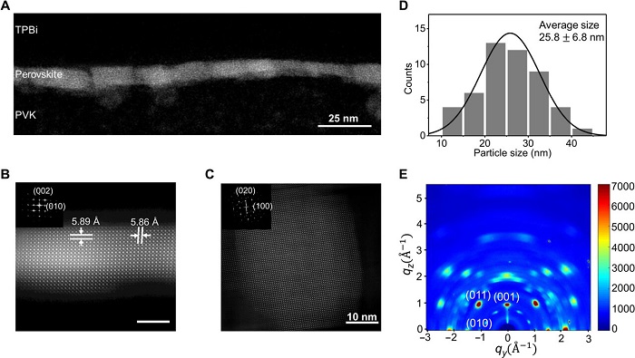
The device contained a perovskite layer analyzed by aberration-corrected scanning transmission electron microscopy (STEM). The team deposited the perovskite film from a precursor solution containing several compounds including lithium bromide, cesium bromide and lead bromide dissolved in dimethyl sulfoxide (DMSO). Thereafter, using high-angle annular dark-field (HAADF) images, Cui et al observed a smooth perovskite film. Using zoom-in studies they noted well-resolved atom columns with highly crystalline perovskite nanoplatelets. Thereafter, using atomic force microscopy, they determined the roughness of the material and understood the size of the perovskite crystals or nanoplatelets using high-resolution transmission electron microscopy.
The team influenced the electronic and optical properties of the perovskite film using the quantum confinement effect and then quantified the orientation of transition dipole moments of the perovskite film. Thereafter, Cui et al. analyzed the light emission of the perovskite film using black focal plane (BFP) spectroscopy. To accomplish this, they probed a small region of the perovskite nanoplatelet film with a laser for photoexcitation. The data indicated excellent spatial uniformity of the horizontal orientation of transition dipole moments in the film. The team next used the BFP data of four spots from different regions to show excellent spatial uniformity of the orientations of horizontal transition dipole moments in the films. Due to the concentration of the bulky organic ammonium cations and the presence of lithium bromide in the precursor solution, the perovskite nanoplatelet film oriented with high photoluminescence quantum yields. By doubling the concentration of the bulky organic ammonium cations, Cui et al. formed perovskite films with strong excitonic absorption peaks and credited the horizontal orientation of the nanoplatelets on the flat substrates to Van der Waals interactions.
Characterizing the room temperature–operating perovskite LEDs
Based on further experiments, the team showed how the introduction of lithium bromide (LiBr) in the precursor solution improved the photoluminescence quantum properties of the film. Additionally, the electroluminescence spectrum of the perovskite nanoplatelet film indicated ultrapure green emissions and the pin-hole free morphology of the nanoplatelet film allowed negligible current leakage. When they performed optical simulations on the materials by using the classical dipole model developed for planar microcavities, the results indicated high-outcoupling efficiency of 31.1 percent for the perovskite devices based on the orientation of the nanoplatelet film. While previous work aimed to control the orientations of transition dipole moments by focusing on the assembly of anisotropic colloidal nanostructures, high-efficiency electroluminescence required the syntheses of anisotropic colloidal nanostructures with high quantum yield. The potential to fulfill the device requirements were challenging due to material design and assembly requirements.
Outlook
In this way, Jieyuan Cui and colleagues showed how the orientation of transition dipole moments of perovskite films could be regulated to overcome the limits of light-outcoupling of planar LEDs to form green LEDs with exceptionally high external quantum efficiency of up to 23.6 percent. The chemical versatility of the perovskite materials allowed Cui et al. to extend the facile approach to in situ grown nanoplatelet films to develop differently colored LEDs with high external quantum efficiency. The work describes a simple and effective method to understand the role of the anisotropic optical properties of nanostructures in the formation of optoelectronic devices.