

Defect inspection scientists from Huazhong University of Science and Technology, Harbin Institute of Technology, and The Chinese University of Hong Kong make a thorough review of new perspectives and exciting trends on the foundation of former great reviews in the field of defect inspection methods. The review focuses on three specific areas: (1) the defect detectability evaluation, (2) the diverse optical inspection systems, and (3) the post-processing algorithms.
The Nanoscale and Optical Metrology Research Center (NOMRC) led by Prof. Shiyuan Liu and Prof. Jinlong Zhu from Huazhong University of Science and Technology and their collaborators from Harbin Institute of Technology and The Chinese University of Hong Kong wrote the first systematic review to introduce the research background, discuss the latest progress and the trend of optical wafer defect inspection. This review has disclosed that cutting-edge techniques such as nanophotonics, optical vortices, computational imaging, quantitative phase imaging, and deep learning can make a profound impact on sub-10 nm defect inspection. The work may pave new avenues for the field of semiconductor wafer defect inspection.


Prof. Jinlong Zhu and Prof. Shiyuan Liu say that “the ever-shrinking features and space on patterned wafers would dramatically strain the capabilities of all the current metrology and inspection solutions in balancing sensitivity, specificity, process speed, and capture rate.”
Optical far-field wafer inspection remains one of the workhorses for defect inspection in the fab. In a conventional defect inspection tool, the defects are captured by comparing circuit pattern images of adjacent dies. The first author of the review article, Prof. Jinlong Zhu says that “the key to defect inspection is not resolution, but the signal-to-noise ratio (SNR) and contrast. The improvement of SNR and contrast highly depends on sophisticated instruments, advanced modeling architectures, and post-processing algorithms, all of which drove us to make a comprehensive review of wafer defect detection methods from the following three aspects: (1) the defect detectability evaluation, (2) the diverse optical inspection systems, and (3) the post-processing algorithms.”
“It is of great importance to carry out defect detectability assessment for a specific type of inspection tools for advanced nodes,” co-first author Dr. Jiamin Liu explained. “In fact, the evaluation of defect detectability usually involves the formulation of quantitative rules for the SNR of the defect scattering signals, the development of simulation tools for defect scattering signals modeling, and the analysis of defect SNR. We found the defect SNR depends significantly on material and defect topology.”
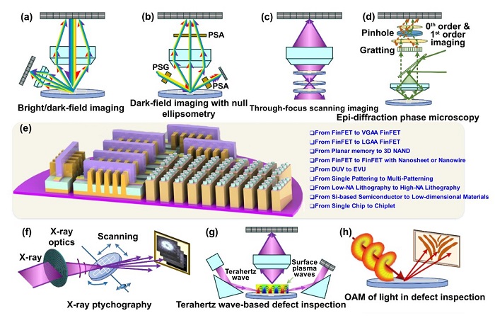
The conventional approaches in optical defect inspection, such as the amplitude-based one alongside its post-processing algorithms, have been thoroughly discussed. The novel inspection mechanisms including phase-, orbital angular momentum-, terahertz wave-, and hyperbolic Bloch modes-based ones, have been highlighted to remind readers of their potentials in opening up new directions in the field. Besides, X-ray ptychography, the only optical method that can directly image both surface and undersurface sub-20 nm defects for the entire wafer, has also been reviewed and prospected in detail in the article. X-ray ptychography has the potential to penetrate the field by providing revolutionary 3D resolution and sensitivity once the drawbacks include the synchrotron X-ray light source, a massive amount of data, and the low speed being conquered in the future.
“Whether it is the simplest image difference operator or the complex image synthetic algorithm or even the deep learning algorithms, these post-processing algorithms play a critical role in optical defect inspection in terms of improving SNR and contrast of defects. Therefore, we provided a detailed discussion of post-processing algorithms involved in patterned wafer defect inspection with a specific focus on the advantages and disadvantages of deep learning algorithms.
Prof. Jinlong Zhu says that they “do believe that optical defect inspection on patterned wafers will remain a challenging but interesting topic that urgently needs to be addressed.