


The new LT 6202 op amp combines 100MHz gainbandwidth, 1.9nV/√Hz voltage noise and rail-to-rail inputs and outputs, while consuming only 2.5mA. It also features a low 0.75pA/√Hz current noise, and it contributes exceptionally low total noise and distortion power in small-signal applications. The device is fully specifi ed on 3V, 5V and ±5V supplies and is available in commercial and industrial temperature grades in both the SOT and SO packages. Dual and quad versions are also available as the LT6203 and LT6204, respectively.
Low Power, 2.4nV/√Hz, Photodiode AC Transimpedance Amplifier Outperforms Monolithic Solutions


You can’t optimize for everything. Op amp designs that try to squeeze good JFETs into their high speed monolithic processes inevitably compromise other parameters, usually resulting in high supply currents. Figure 1 shows a simple way to get the best of both worlds using the LT6202 and a low noise discrete JFET. The JFET acts as a source follower, buffering the inverting input of the LT6202 and making it suitable for the high impedance feedback elements R1 and R2.
The LT6202 forces the JFET source to 0V, with R3 ensuring that the JFET runs an IDRAIN of 1mA. Because the JFET is run well below its minimum IDSS and has a narrow range of pinchoff voltages, the circuit is guaranteed to self bias just below ground, typically at about –0.5V. Without a photocurrent signal in the photodiode, the LT6202 output sits at the same voltage and tracks it. When the photodiode is illuminated, the current must come from the LT6202 output through R1 and R2 so the output goes up as it would with a normal transimpedance amplifier.
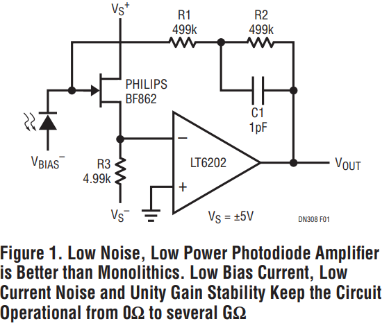 Amplifier input noise density and gain-bandwidth product were measured to be 2.4nV/√ Hz and 100MHz, respectively, with only 3.8mA supply current. This is unparalleled in the monolithic world where 5 to 6 times the supply current would be expected for similar performance. The 100MHz gain-bandwidth product of the LT6202 is maintained in this circuit because the JFET has a high gm, approximately 1/80Ω, which looks into 4.99kΩ so its loop attenuation is less than 2%.
Total circuit input capacitance including board parasitics is measured at 3.5pF. This is less than the specifi ed CGS of the JFET because the JFET source is not grounded but rather looks into R3 and the high impedance op amp input. This fact combined with the low input voltage noise makes the circuit well suited to both large and small photodetectors. Using a small photodiode with 2.5pF junction capacitance and adjusting parasitic feedback capacitance for 4% overshoot in the transient response, closed loop bandwidth is 1.6MHz.
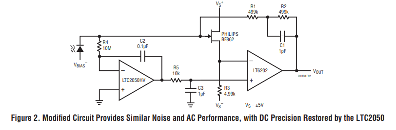
Figure 2 shows the LT6202 applied in a manner very similar to that shown in Figure 1. In this case however, the JFET is not allowed to dictate the DC bias conditions. Instead of simply grounding the LT6202 non-inverting input, an LTC2050 drives it (and therefore the source) exactly to where it needs to be for zero JFET gate voltage. The addition of the LTC2050 increases the total supply current by about 1mA. AC performance is nearly identical to the uncorrected circuit of Figure 1, with the additional benefi t of excellent DC performance. Output offset is 200μV and output noise is 2mVP-P measured in a 20MHz bandwidth.
 Single Supply 16-Bit ADC Driver
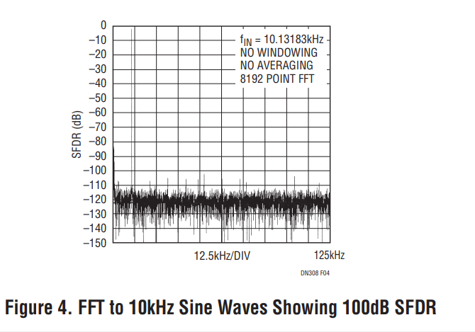
Figure 3 shows the LT6203 driving an LTC1864 unipolar 16-bit, 250ksps A/D converter. The bottom half of the LT6203 is in a gain of 1 and buffers the 0V negative full-scale signal VLOW into the negative input of the LTC1864. The upper half of the LT6203 is in a gain of 10, referenced to the buffered voltage VLOW and drives the positive input of the LTC1864. The input range of the LTC1864 is 0V to 5V so for best results the input range of VIN is from VLOW, about 0.4V to about 0.82V. Figure 4 shows an FFT obtained with a 10.1318kHz (coherent) input waveform, with no windowing or averaging. Spurious free dynamic range is seen to be 100dB.
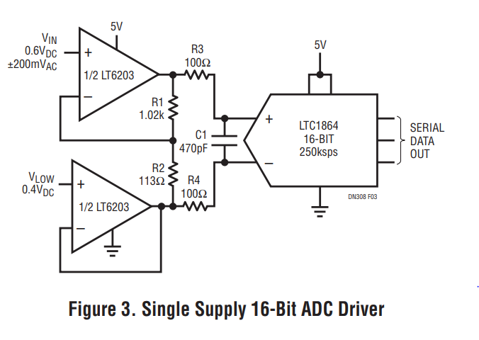 Although the LTC1864 has a sample rate far below the gain bandwidth of the LT6203, using this amplifier is not necessarily a case of overkill. A/D converters have sample apertures that are extremely narrow (infinitesimal as far as mathematicians are concerned) and make demands on upstream circuitry far in excess of what the innocent looking sample rate would imply. In addition, when an A/D converter takes a sample, it applies a small capacitor to its inputs causing a fair amount of glitch energy and expects the voltage on the capacitor to settle to the true value very quickly. Finally, the LTC1864 has a 20MHz analog input bandwidth and can be used in under sampling applications, again requiring a source bandwidth and settling speed higher than the Nyquist criterion would imply.
Conclusion
The LT6202, LT6203 and LT6204 are fast, low noise amplifiers which have been optimized for low power consumption. Their rail-to-rail inputs and outputs provide fl exibility and ease of use and maximize dynamic range.
Courtesy: www.analog.com