

This application note considers off-data-sheet operation of integrated circuits (ICs). It discusses the pitfalls awaiting engineers who have not experienced Murphy’s Law, which is anything that can go wrong, will go wrong at the worst possible time. The article reviews the thought process of an experienced and inexperienced engineer, and how they can make a circuit immune to leakage from environmental contamination, radio frequency interference, and electro static discharge.
Introduction
I believe in Murphy’s Law as a general rule in life.


Murphy’s Law says that anything that can go wrong, will go wrong at the worst possible time. Wikipedia illustrates the history of Murphy’s Law with the image shown in Figure 1. Murphy sometimes produces train wrecks.
Wikipedia explains that the 1895 derailment occurred when the Granville-Paris Express overran the buffer stop. The accident was caused by a faulty brake and the engine drivers who were trying to make up for lost time. The engine careened across almost 30m (98ft) off the station concourse, crashed through a 60cm (24in) thick wall, shot across a terrace, sailed out of the station, and plummeted onto the Place de Rennes 10m (33ft) below, where it stood on its nose. For much more on Murphy’s Law see: Murphy’s laws site.

Standard Device Testing and Data Sheet Specifications
Consider now how Murphy’s Law can affect ICs that have been tested and meet published specifications. It is important to understand that there is a difference between the way an IC is tested and the way the IC is used in a customer’s application. Test time on the automatic test equipment (ATE) is very costly; it is paid for in portions of a second. Since there are usually many possible applications for an IC and just one test, the manufacturer sets specifications to meet the majority of the applications. Then a test procedure is defined to test those specifications with minimum test time. A well-known adage of the IC industry says that: the data sheet describes the test conditions and specifications. All manufacturers guarantee that the part meets the minimum and maximum values by a combination of tests and/or simulation (this is what is meant by “guaranteed by design.”).
An example of a parameter that is commonly “guaranteed by design” is the operating temperature range. The part is tested at one temperature, “room,” meaning +25°C; it is not tested for every temperature in the device’s published operating range. Rather, design simulation allows us to predict the device’s operation over the whole range of temperature and process variations. Most manufacturers, moreover, set guardbands around the parameters to allow for these variations. Statistically many manufacturers set a safety wall at “six sigma,” a commonly accepted way to state that the standard deviation has a 99.9997% probability of meeting the specification for that parameter. Guaranteed by design is used for the operating temperature range instead of increasing test time by three times or more.
How Can a Part Be Used “Off Data Sheet?”
All parts have limitations. We just cannot design a single part for all possible uses. Even if someone tried, no one could afford to pay for such a part. That is why there are literally thousands of logic parts and device families as well as operational amplifiers (op amps) and analog-to-digital (ADC) and digital-to-analog (DAC) data converters.
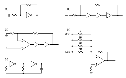
To illustrate, some years ago CMOS (complementary metal oxide semiconductors) logic was invented. It was designed to be inexpensive digital logic. Engineers soon started using the digital logic in a linear analog way for the endless applications that would benefit from less expensive IC devices. In Figure 2a a logic inverter with two resistors is used as a crude amplifier. The specifications of the resulting device are barely good enough to work. The data sheet says nothing about this application, and the IC manufacturer does not guarantee any parameters for this use. Thus this crude amplifier is, in fact, the definition of “off-data-sheet” use. Clever engineers could use all six inverters in the IC package. Figure 2b adds larger current-drive capabilities to an op amp. While Figure 2c is an oscillator, Figure 2d is the same as Figure 2a with more gain. Figure 2e is a 4-bit DAC. If we drive Figure 2e with a counter, we get a staircase generator. Add a windowed comparator and we can make a successive-approximation ADC by stopping the counter when the DAC output matches the incoming voltage.
Sometimes new industry-standard or customer-specific products evolve from off-data-sheet use. A customer might want a certain parameter guaranteed and approaches the manufacturer : “We will pay a little more if you test x and y. We will buy a million pieces this year”. As for new products, a standard logic family once used emitter-coupled logic (ECL). It was faster than most in its day because the transistors operated in a linear mode (music to the analog engineer’s ears) instead of the slower saturated switching transistors. The first customers and applications used ground and a negative power supply. Not only were engineers trying it in analog circuits, they used it with a ground and a positive power supply. A new product family resulted with the obvious name PECL for positive emitter-coupled logic.
Sometimes parts are misused in off-data-sheet applications. Parts maybe over-clocked; they are run at speeds in excess of that guaranteed by the data sheet. The parts may be run hot on purpose because the customer is willing to reduce reliability for a performance advantage. The power supply may be margined, which is a method of varying the supply voltage board by board to either remove marginally poor boards or select the super stars that will command a better price for the performance. All of these uses are acceptable, if the engineer understands the ramifications and understands that the IC manufacturer does not warrant or guarantee such operation.
The Risks of Designing Off Data Sheet
Off-data-sheet use can also trap inexperienced digital designers in circuit designs that simply will not work as envisioned. Some educational institutions are concentrating on digital technology so much that analog education is suffering. As a result, some young bright engineers lack certain knowledge and experience. Modern consumer devices tend to take advantage of digital technology. Unfortunately the human interface involves the analog senses of touch, hearing, and vision. Also power supplies need to be cleaned and filtered in analog ways to isolate circuits from interference and other circuits.
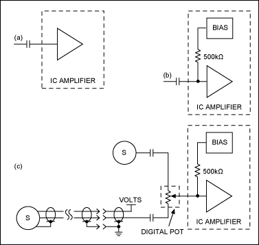
Figure 3 illustrates an analog trap that a new digital engineer can fall into. The experienced analog engineer will see at least three traps waiting because of inattention and the high-input impedance. First, there is the DC issue with leakage; second, there is an electro static discharge (ESD) issue, and third, the AC issue with noise plus radio frequency interference (RFI). We will examine each in turn.
DC Leakage Issues
Figure 3a shows a high-gain (over 40dB; a ratio of 100) amplifier. The IC data sheet cautions that the input capacitor needs to be as close as possible to the input pin. The data sheet also warns against “long” traces on the input pin.
Our new digital engineer may think “OK,” meaning that if the leads are kept under about an inch in length then they are not long and the circuit will function properly. This engineer never envisions Figure 3b. Meanwhile, the experienced analog engineer understands that the AC-coupled (capacitor) amplifier must have its DC bias voltage set in some way. Our analog engineer continues reading the data sheet to see the circuit in Figure 3b. Unfettered by experience, the digital engineer proceeds with the design. There are actually two sensors that need to be attached to the amplifier input, one local on the PCB (PC board) and one external attached through a connector with 3ft to 6ft of wire. While this need would alert the experienced analog engineer, our digital engineer is lulled into complacency by the seemingly simple circuit. Instead of a switch between sources the digital engineer decides to use a remotely controlled digital pot. This allows the fading between the two sensors and simplifies the system as it reduces settling issues at switch time. So does the digital engineer now breadboard the circuits? No, only an old-fashioned engineer would wire and solder a physical breadboard. The new digital engineer lays out the board and assembles it.
Now Murphy’s Law really steps in. Think of the sequence of events through the design cycle. The date for production handoff is set. Every delay during the entire design piles up tasks at the end just before the handoff. Where is our digital engineer most likely to be rushed, sleep deprived, and under pressure? This is always during board test and initial system testing. Now the problematic issues emerge; the “train” hit by Murphy’s Law earlier begins to derail. Thankfully, most issues can be fixed in software and firmware, or at least reduced below the threshold where a common consumer will not notice. The problems do not require the dreaded board relayout. Everything is now working, so system testing continues. Time is short, but the project is functioning smoothly and is released into production. Production builds a pilot run which meets specifications Mass production begins.
The experienced analog engineer fears Murphy’s Law. This is a good respectful fear. As a result our analog engineer starts the project with different expectations. First there must be breadboards, maybe not for all the circuits, which are known from previous projects. Certainly any new state-of-the-art, cutting-edge circuits, which are the features on which this product depends, will get a breadboard. Then this analog engineer will plan on relaying out the board three times to optimize it. Some projects are planned to have even more board layouts. (Note: We can look at the front-end board of an oscilloscope and notice two things. First, the board layout revision number will be 9 or higher and, secondly, the layout is copyrighted. This is because the board layout is an integral and inseparable part of the design.) Our analog engineer will allow time for delay buildup and thorough testing at the board and system level. Testing in the consumer’s operating environment is accommodated.
Why is the experienced analog engineer panicking?
Figure 3c is a disaster. It is asking for Murphy’s Law to strike. Oh, did we mention that this is a consumer product that will be carried in the customer’s pocket? First, we give the digital pot a number so we know its package size. It is a MAX5418, a 256-tap, 100kΩ in a 3mm x 3mm TDFN package; the pot pins are in a row on one side of the part. This part sounds good to the new digital engineer because 3mm x 3mm means the board traces will be short. “Wait, not so fast,” says the analog engineer. With a 500kΩ input impedance, how do we protect against leakage from solder flux residue and a dirty PCB? Even if the PCB is properly cleaned after assembly, how do we protect it from human contamination in its operating environment? Is conformal coating necessary?
When a human breathes in the environment, objects in the area (e.g., in a shirt pocket) will have many compounds deposited upon them. Human breath has moisture (water vapor); metabolic waste like aldehydes and ketones from breaking down carbohydrates, alcohol, acetone, smoke; and smog from the atmosphere (most things that are breathed in, are breathed out). Then if the human can touch the board, there will be fingerprints containing metabolic compounds, sulfuric acid, and oils to collect dust. The human is also continuously sluffing off skin cells and hair particles. These particles attract and hold moisture. Moist dirt conducts electricity.
There is an unintended consequence from the necessity to control ESD during manufacturing. Antistatic devices are used in the IC package assembly, during ATE test, at IC shipping, as well as in the PCB assembly, product test, and shipping. Clothing smocks and lab coats are coated with hydrophilic materials which flake and rub off as the person moves. Many wear conductive booties with sacrificial carbon-loaded trailing straps which shed conductive particles. The equipment may have conductive metal and plastic bristle brushes which wear out, leaving conductive particles. The shipping bags, bubble wrap, and IC reels and tubes all shed conductive hydrophilic particles as the parts shake and rattle in shipment. Hydrophilic materials reduce static buildup by sucking moisture out of the air to make surfaces conductive. Again, moist contamination conducts electricity.
We return to the PCB trace length and the DC leakage.
The op amp is actually the input section of an ASIC. The ASIC is packaged as a ball grid array (BGA); it has more than 50 balls on 0.031in (0.8mm) centers. On the PCB the ASIC is surrounded with an area of confusion. This is where the signals are trying to spread out to make interconnections. If board cost was not a consideration, one would like to increase the number of layers in a PCB near a BGA package. Because the signals are packed so densely it is difficult to fan them out and connect them to the surrounding circuits. Most consumer product PCBs today limit themselves to two or four circuit conductor layers. Toys and other extremely cost-sensitive products can be single-sided PCBs with jumpers. In the case of BGAs four-layer boards require very skillful layout. To begin, the two center layers of circuits are reserved for power and ground planes, respectively. As one nears the ASIC, the ground and power planes need to contain other circuits; the ground and power planes are sacrificed to add the signal paths. Even using all four layers, the job of connecting the circuits is difficult. Some signals may need to stitch from layer to layer multiple times to route. Because each stitch through a via adds inductance, the lowest frequency must be stitched first.
Another concern is that the input ball is adjacent to a power ball. Before soldering, the balls are 0.013 inches apart; the distance after soldering depends on the PCB trace dimensions. In any case, there is a potential for flux, dirt, hydrophilic or other contamination to cause leakage current here.
The new digital engineer will look at Figure 3c and propose to get the trace between the ASIC input and the pot’s wiper down to about 0.078in (2mm). The experienced analog engineer will look for DC leakage and conclude that the pot’s high and low pins, as well as two capacitors are connected. Why? Because in use, the pot’s wiper is usually connected to one end while the other end connected through 100kΩ is still in the circuit—as we will see. Returning to the DC case, we estimate that trace distance between the pot ends and the two capacitors adds 0.2in (5mm). That means that any leakage current from flux, dirt, or contamination over 0.275in of board trace and on the surface of the two IC packages can cause leakage currents. The circuit thus fails if the ASIC bias voltage changes by 5mV. Ohms law says that 5mV over the 500kΩ input impedance is 10nA. How much flux, dirt, or hydrophilic contamination is required to leak 10nA? From very little to almost none will cause leakage.
The ESD Issue
We have an external pin connected to our 500kΩ circuit impedance. Murphy’s Law is calling—how do we protect against ESD? If the consumer walks across a rug in a low-humidity situation, rubs their clothing on a vinyl chair, or pets the cat, they generate static electricity. Then just plugging in the cable to the product’s external connector will produce in-field failures. We are talking arcs with enough power to ionize the air. When we see an arc, we are seeing the air super heated to incandescence.
When one walks across a carpet on a low-humidity winter day, a static charge can build up. The charge is discharged suddenly when we touch a metallic object and it hurts us. Arcs a centimeter (0.4in) long are not uncommon. A general rule is that a 1cm spark is 5000V in 50% relative humidity air.
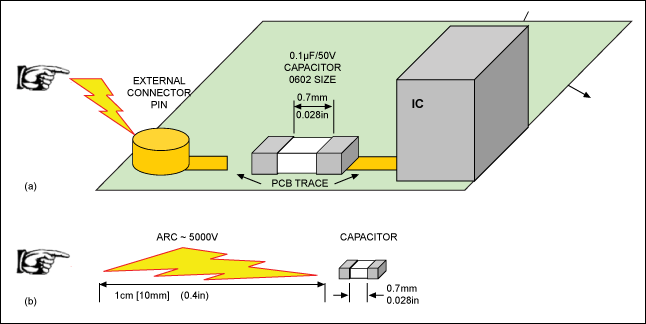
ESD hurts capacitors and ICs too! Figure 4a shows the circuit designed by our new digital engineer, who feels safe because no DC path exists from the outside connector to the IC. However, after spark has jumped 0.4in, it easily jumps 0.028in. Figure 4b has the external arc and the capacitor drawn at the same scale. This is a giant lightning bolt inside the IC, where spacing are less than the width of a human hair. After the first arc the capacitor could short as it is only specified to have a 50V working voltage. The IC is, at best, only slightly damaged. In a worst-case scenario, it is destroyed and the lightning bolt may have propagated through the first IC destroying other ICs on the board.
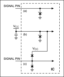
To protect ICs from ESD, almost all have ESD-protection structures on the pins. Figure 5 is a simplification of such ESD structures.
If a lightning bolt hits or comes close to a power line, there is so much energy that nothing survives. The safest thing to do if a lightning storm approaches is to unplug electronic appliances. ESD structures inside an IC are not designed to cope with lightening strikes. They are, instead, designed to dissipate the minor environmental static that can occur from metallic machine and human body contact. The most important time to protect the IC is before it is soldered to the PCB. This is during the IC package assembly, ATE test, and IC shipping, as well as in the PCB assembly; antistatic devices are used throughout these processes. Special clothing, wrist straps, shoe discharge straps, as well as equipment designed to reduce static are common. ESD protection is so critical to the end product reliability that the effectiveness of the ESD equipment is tested at least daily.
Picture the IC in Figure 5 before it is soldered to a PCB. There is nothing connected to the external pins. The object is to homogenize the static electrical charge across the IC so that no current flows. This is just like flying a satellite in space; we do not know or care what the static charge is until we come in contact with some other object. A tube or reel of ICs is in the same condition. As long as the static charge is uniform no current flows, which is why the tubes and reels are electrically conductive. When a tube or reel is received from a shipment, the static is discharged on a conductive grounded table. Once the container is at the same local ground potential, the ICs can be removed from the container. Have you ever watched one engineer deliver bare ICs across the lab to another engineer? They know that if they were to hold one end of an IC and allow the other end to contact the other engineer or grounded table top, they may discharge the static through the IC. The discharge current could destroy the IC. Actually, both engineers touch the same conductive table top before transferring the ICs. Or the engineers can touch hands to equalize any static charge before transferring the ICs.
If a conditions occurs where current flows inside the IC, the Zener diodes in Figure 5 a and b will conduct in the forward and backward directions to minimize the damage. The circuit in Figure 5c will cause the bottom diode to conduct for negative voltages. For positive voltages, the upper diode will be forward biased and the zener diode on the VCC line will conduct in the reverse bias direction to try to protect the IC.
Now picture the IC in Figure 5 soldered to the PCB. The IC is usually better protected on the board than when compared to the unmounted condition. Most experienced analog engineers’ circuit-board designs incorporate their own ESD protection for the board’s external connections. The board’s ESD protection can include devices and technologies that carry larger voltages and currents than are possible to build inside ICs. PCBs are protected from ESD by a combination of discrete diodes, avalanche diodes, transient-voltage-suppression (TVS) diodes, gas tube discharge devices, resistors, inductors, and metal oxide varistors (MOVs), to name a few. The external discrete components are larger, and provide more robust board ESD protection between the external connector and the ICs. The Figure 5 IC then needs only to handle modest residual ESD; the protection circuits of a, b, and c will then operate as above in the unmounted condition with the board circuits providing low-impedance paths for VCC and other pins.
Under catastrophically large ESD conditions, the entire ESD structure and IC will be destroyed. Removing the top of the integrated circuit by decapping will show what looks like a lightening bolt hit the chip. We will see everything from tiny pinhole burn marks to what was a molten mess. If there is just a tiny ESD event the ESD diodes may start to leak. These leakages could start with pico- and nano-amp currents. As further ESD events occur, the leakage can increase; other damage can also degrade the performance of other devices inside the IC. This deterioration reduces the reliability of the IC and any product that use it. This is the reason that we need to take ESD protection at every step.
RFI and PCB Trace Length
Household microwave ovens, WiFi, cordless phones, and Bluetooth® radios operate around 2.4GHz; the wave length is just under 5in. Antennas, whether planned or unintentional, have good gain when they are ~1/8 wave length or longer. One-eighth wavelength for 2.4GHz is 0.6in (10.5mm); for 5.7GHz cordless phones it is 0.26in (6.6mm). Cell phones operate at various frequencies; at 1.8GHz a 1/8 wave is 0.82in (21mm) and at 800MHz a 1/8 wave is 1.85in (47mm). Remembering these wavelengths, we return to the PCB trace lengths and look at Figure 3c. The AC signals are induced into the traces, and can go through the capacitors or other stray circuit capacitance. We estimate that the traces without any external cable attached (but including the connector pins) are 0.24in (6mm) minimum. “That is good,” the new digital engineer says. The experienced analog engineer mumbles, “We should calculate the field strength of the cell or cordless phone when it is one foot away. This 0.6W or more is not that simple.” Our digital engineer is happy, while the analog engineer continues testing for the “real-world” issues that the customer will face in the field. Our analog engineer knows that the RFI will be rectified in the early stages of the ASIC and cause problems. The analog engineer then connects an external cable. Good cables specify the percentage of shield coverage with frequency. A good cable can function, but what happens if the external connected sensor ground wire frays with wear? What happens when someone substitutes a less expensive or unshielded cable? What if the ground-wire shield is leaky at the frequency of interest? What happens when the connector gets dirty or loose? We can have in-field failures. Is that acceptable in this design? Our experienced analog engineer decides to protect the front-end with a lowpass filter. The new digital engineer never knows that there is possibility of danger.
Why Does the ATE Not Catch Small nA and pA Leakage?
The new digital engineer may wonder why the ATE does not test every possible thing that might be encountered in a field application. Return to the comments above under Standard Device Testing. First, if “the thing” is not a data sheet parameter, the ATE is not looking. Second, much of the cost of the IC is determined by test time, so customers do not want to pay for testing just because someone wants to use the part off data sheet.
The Circuit Solution: the Small Changes Necessary to Protect The Product
The MAX5418’s data-sheet Electrical Characterization table says that the pot’s high pin is connected to V
CC and that the pot’s low pin is connected to ground. The leakage can not be measured in this condition. The pot’s wiper is connected to the ends. If connected to either end, the wiper is connected to ground or VCC through the few hundred ohms of the wiper’s resistance. (Note: no leakage reading is practical.) If the pot is midrange the wiper sees two 50kΩ resistors in parallel. Therefore:
10nA × 25kΩ = 0.25mV offset
(This is something that the ATE does not look for, and is tolerated in most well-designed circuits.) Even in pins where leakage is measured most manufacturers set 1µA as the acceptable limit. Figure 6 shows a proper circuit design. Even a 1µA leakage on the MAX5418 portion of the circuit would be ignored and have no effect.
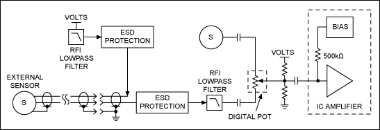
In Figure 6 the external sensor input is protected from RFI and ESD. The new digital engineer might ask: “Why does the VCC line need protection? Is it an outgoing line?” For ESD and RFI the VCC line is actually bidirectional. How will all other the circuits operate with ESD and RFI propagated on the VCC line? They will probably operate poorly. What about the internal sensor? Will it need ESD and RFI protection? That will depend on what the sensor is and how it is constructed. Could an external arc strike the sensor through a hole in the outer insulating case? Is the outer surface of the sensor grounded, thereby protecting its signal output port? These and many more things need to be considered by the designer. It has long been true—experience helps us do a better job.
Between the pot and the ASIC there is a capacitor. To the left side of the capacitor the two resistors set the pot’s bias. The resistors will be set in the low kΩ range to wash out any DC leakage. The exact resistor value will be determined by the sensor impedance and power drawn. In fact, since the capacitor blocks the DC to the ASIC input, even much large leakage currents are ignored. Note that the circuit trace on the right side of the capacitor between the capacitor and IC amplifier (ASIC) is as short as possible, just as the ASIC manufacturer recommends. This ASIC input still sets it own bias and it has a 500kΩ impedance. This makes it sensitive to dirt and contamination, but it is now a very small area, thus minimizing the risk. To have the best confidence in the reliability, one should consider a conformal or an epoxy coat over this small area.
Conclusion
Murphy’s Law is always lurking during circuit design, and it always brings the usual unexpected bad results for the inexperienced engineer. Murphy’s Law is particularly active with off-data-sheet designs. In the end, knowledge and experience are the best way to forestall Murphy and his Law.
The Bluetooth word mark and logos are registered trademarks owned by Bluetooth SIG, Inc. and any use of such marks by Maxim is under license.
Article courtesy: www.maximintegrated.com