


Description
The TIDA-01021 design is capable of supporting two high-speed channels on separate boards by using TI’s LMX2594 wideband PLL with integrated VCOs to generate a 10-MHz to 15-GHz clock and SYSREF for JESD204B interfaces. The 10-kHz offset phase noise is < –104 dBc/Hz for a 15-GHz clock frequency. This TI Design uses TI’s ADC12DJ3200 high-speed converter EVMs to achieve a board-to-board clock skew of < 10 ps and an SNR of 49.6 dB with a 5.25- GHz input signal. All key design theories are described, guiding users through the part selection process and design optimization. Finally, this reference design presents schematics, board layout, hardware testing, and results.


Features
- Up to 15-GHz Sample Clock Generation
- Multichannel JESD204B Compliant Clock Solution
- Low-Phase Noise Clocking for RF Sampling ADC and DAC
- Configurable Phase Synchronization to Achieve Low Skew in Multichannel System
- Supports TI’s High-Speed Converter and Capture Cards (ADC12DJ3200EVM, TSW14J56, and TSW14J57)
Applications
- High-Performance Oscilloscopes
- Phased Array Radars
- Wireless Communication Testers
- Direct Sampling Software Defined Radio
 1 System Description
Clocking solutions for high-speed GSPS direct RF sampling signal chains are critical to achieve high SNR and low channel-to-channel skew. This reference design demonstrates a multichannel phase synchronized clocking platform that can be used in applications such as DSO, phased array radars, and 5G wireless testers. Using the LMX2594 frequency synthesizer for DEVCLK and SYSREF generation, this TI Design can clock JESD204B data converters. Furthermore, by using the LMK04828 to generate the FPGA clocks and SYSREF signals, multiple channels can be supported.
In this solution, two LMX2594 devices receive a 100-MHz VCXO reference signal through the LMK04828 and generate phase synchronized DEVCLK (sampling clock) and SYSREF for two high-speed signal chains. The LMK04828 clock jitter cleaner generates independent SYSREFREQ signal and SYNC signal to both LMX2594 devices for SYSREF generation. The LMK04828 generates FPGA device clocks for each channel that are synchronized to the respective SYSREFREQ outputs.
High-performance multichannel digital storage oscilloscopes require a signal chain with a wideband analog front end, high SNR, and low channel-to-channel skew. The ADC12DJ3200 ADC is well suited for these requirements. The clocking solution described in this TI Design provides an optimum solution for clocking the ADC12DJ3200 ADCs to achieve high SNR and low channel-to-channel skew.
Wireless tester equipment use multichannel receivers for testing cellular and MIMO devices. Wireless testers require high dynamic range and wideband receivers to test 3G and later wireless standards-compliant equipment. The ADC12DJ3200 is well suited for the multichannel receiver requirements of the wireless testers. The clocking solution described in this TI Design supplements a high-performance signal chain solution based on multiple ADC12DJ3200 ADCs to achieve a low time skew between channels providing both high dynamic range and wide receiver.
Phased array radar applications need a high dynamic range, wide receiver bandwidth, low latency, and good synchronization between the channels. The signal chain solution based on the LMX2594, ADC12DJ3200, and LMK04828 devices are able to achieve optimum performance for phased array radar applications.
Direct RF-sampling software-defined radio (SDR) technology needs multiple channels, high dynamic range, highly re-configurable receiver bandwidth, and wide input frequency range. This TI Design can meet the requirements of the high-performance SDRs in terms of multichannel, dynamic range, and reconfigurability.
1.1 Key System Specifications
The objective of the TI Design is to demonstrate a high-speed clocking solution for a multichannel signal chain. Phase noise and jitter performance of the LMX2594 along with an onboard crystal or LMK61E2 reference is shown in Table 1. The TIDA-01021 design focuses on measuring the SNR at the
ADC12DJ3200 signal chain and configurable phase delay to align multichannel clocks. The data capture is done by the TSW14J56, which is interfaced with the ADC12DJ3200EVM using an FMC adapter card.
Table 1 lists the key system level specifications for the signal chain from the clocking solution perspective.
Table 1. Key System Specifications
| PARAMETER | SPECIFICATIONS | CONDITIONS |
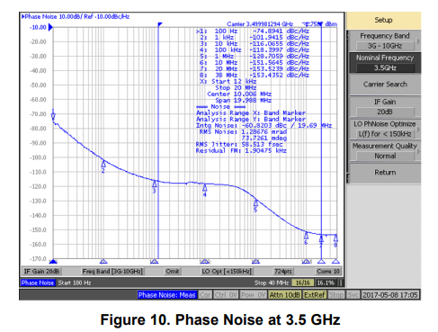
| Dev_Clk phase noise | –117.0 dBc/Hz at 10-kHz offset
–119.7 dBc/Hz at 100-kHz offset –130.5 dBc/Hz at 1-MHz offset –149.5 dBc/Hz at 10-MHz offset |
at 3.5 GHz |
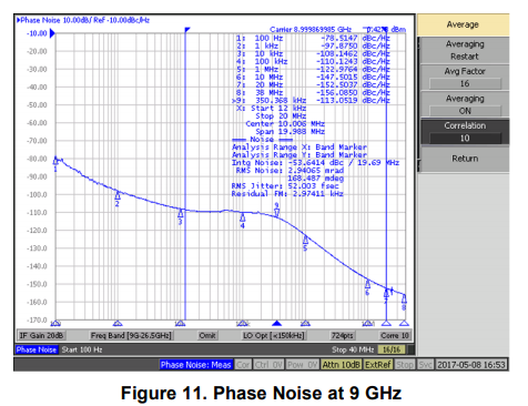
| –108.8 dBc/Hz at 10-kHz offset
–111.4 dBc/Hz at 100-kHz offset –123.1 dBc/Hz at 1-MHz offset –147.4 dBc/Hz at 10-MHz offset |
at 9 GHz | |
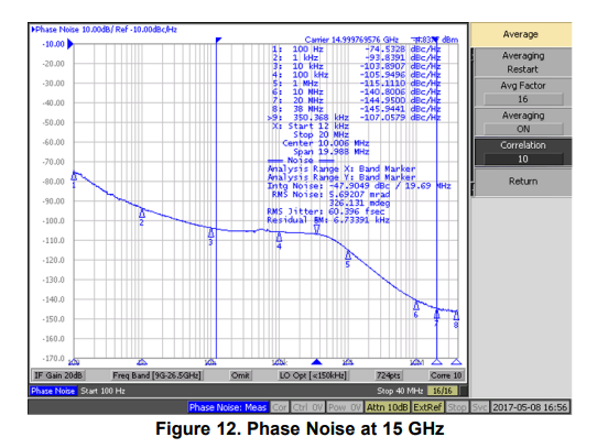
| –104.7 dBc/Hz at 10-kHz offset | ||
| –107.5 dBc/Hz at 100-kHz offset
–114.7 dBc/Hz at 1-MHz offset –141.7 dBc/Hz at 10-MHz offset |
at 15 GHz | |
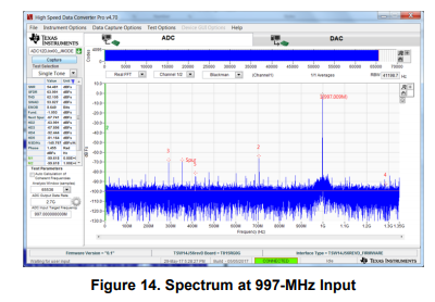
| SNR (dBFS) (dual channel mode) | 56.3 | at a 997-MHz ADC input signal |
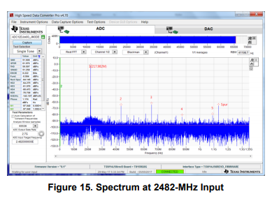
| 55.2 | at a 2482-MHz ADC input signal | |
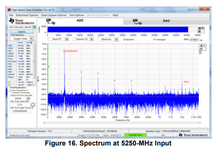
| 52.6 | at a 5250-MHz ADC input signal | |
| Multichannel clock time skew | < 10 ps | at a 3-GHz clock output |
| Channel-to-channel time skew | < 50 ps | at a 997-MHz ADC input signal |
| at a 2482-MHz ADC input signal |
Overview
2 System Overview
2.1 Block Diagram
Figure 1 shows the block diagram of the high-speed multichannel clock solution interface with the ADC12DJ3200 EVM and TSW14J56 capture cards. The ADC12DJ3200 EVM is interfaced with the TSW14J56 data capture board through an FMC+ adapter board. The ADC DCLK and SYSREF are provided from the TIDA-01021 clocking board using the length matched cables.

System Overview
2.2 Highlighted Products
2.2.1 LMX2594
The LMX2594 is a high-performance, wideband RF PLL with integrated VCO that supports a frequency range from 10 MHz to 15 GHz without using an internal doubler. The device supports both fractional-N and integer-N modes, with a 32-bit fractional divider allowing fine frequency selection. The high-performance PLL with a figure of merit of –236 dBc/Hz and high phase detector frequency can attain very low in-band noise and integrated jitter. Its integrated noise of 45 fs for a 7.5-GHz output makes the device an ideal low-noise source.
The device accepts an input reference frequency up to 1.4 GHz, which combines with frequency dividers and programmable low-noise multiplier to allow for flexible frequency planning. The high-speed N-divider has no pre-divider, thus significantly reducing the amplitude and number of spurs. The additional programmable low-noise multiplier allows users to mitigate the impact of integer boundary spurs. In fractional-N mode, the device can adjust the output phase by a 32- bit resolution.
For applications that need fast frequency changes, the device supports a fast calibration option, which takes less than 20 μs. The LMX2594 adds support for generating or repeating SYSREF (compliant to JESD204B standard), making it an ideal low-noise clock source for high-speed data converters. Fine delay adjustment (9-ps resolution) is provided in this configuration to account for delay differences of board traces. This device uses a single 3.3-V supply and it has integrated LDOs that eliminate the need for onboard low-noise LDOs.
2.2.2 ADC12DJ3200
The ADC12DJ3200 is a RF-sampling GSPS ADC with a –3-dB input bandwidth up to 6 GHz. The 12- bit ADC12DJ3200 can sample up to 3200-MSPS in dual mode and up to 6400-MSPS in single channel mode. The ADC12DJ3200 can be used to sample signals in the first, second, and higher Nyquist zones. The ADC12DJ3200 use a high-speed JESD204B output interface with up to 16 serialized lanes and supporting subclass-1 for deterministic latency and multi-device synchronization. The serial output lanes support up to 12.8 Gbps and can be configured to trade off bit rate versus number of lanes. In dual channel mode, optional digital down converters can tune and decimate a band from RF to a complex baseband signal to reduce the interface data rate in bandwidth limited applications.
2.2.3 LMK04828
The LMK04828 is a dual-PLL jitter cleaner and clock generator for JESD204B systems. The LMK04828 has 14 clock outputs from PLL2 those can be configured drive seven JESD204B converters or other logic devices using device and SYSREF clocks. The LMK04828 supports two ranges of VCOs, from 2370 to 2630 MHz and 2920 to 3080 MHz.
2.2.4 LMK61E2
The LMK61E2 is an ultra-low jitter PLLatinum programmable oscillator with a fractional-N frequency synthesizer with an integrated VCO that generates commonly used reference clocks. The outputs can be configured as LVPECL, LVDS, or HCSL. The device features self-startup from an on-chip EEPROM that is factory programmed to generate a 100-MHz LVDS output. The device registers and EEPROM settings are fully programmable in-system through an I2C serial interface. Internal power conditioning provides excellent PSRR, reducing the cost and complexity of the power delivery network. The device operates from a single 3.3-V ± 5% supply. The device provides fine and coarse frequency margining options through I2C serial interface to support system design verification tests (DVT) such as standard compliance and system timing margin testing.
1.1 System Design Theory
The multichannel clock design is based on two design goals: low-phase noise DEVCLK generation and scalable multichannel clock solution with provision for phase alignment trimming. This section describes the design details of various functional blocks that help to achieve these system design goals.
1.1.1 LMX2594 Improved Phase Noise
The TIDA-01021 block diagram is shown in Figure 2. In order to achieve phase synchronization, the two LMX2594 synthesizers are given a common reference frequency input, SYNC and SysRefReq signal from the LMK04828. To adjust slight mismatches in phase of the two generated clocks, the LMX2594 provides the feature of programming the clock phase using the MASH_SEED value. From the LMK device, the OSCout signal provides the reference frequency to the LMX2594. The SDCKout signal is used for generating sync and sysref for the LMX2594. Because the LMX2594 devices are being used in master mode, SysRefReq signal needs to be at logic high. To ensure this, the respective SDCLKout pins are made conditionally low. Prior to feeding this signal to a balun, the positive and negative signals of the differential pair are exchanged. This exchange gives a continuous high logic at the balun output and serves as the SysRefReq signal.
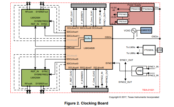 A positive edge is required at the sync input to force the LMX2594 devices in sync mode. By toggling the SYNC_POL bit, the LMX2594 device is brought into the sync mode first. This process also enables the SDCLKout outputs and starts sending pulses to the sync pin. Because the SDCLKout pins used for sysref are conditionally low always, they are not affected by this operation. Once a pulse has been provided to the sync pins of the LMX devices, the respective SDCLKout pins are powered down.
The LMK04828 provides a clock of 100 MHz from OSCout to the LMX devices, which is then converted to 200 MHz inside the device and used as the phase detector frequency. Higher phase detector frequency improves the phase noise and also avoids spurs. As a result, loop filters are designed for a 200- MHz phase detector frequency. For this TI Design, the phase noise of the output clock is the critical performance parameter. Its measurement results are given in Section 4.
1.1.2 Multichannel Configured Phase Synchronized Clocks
When clocking multiple channels, channel-to-channel skew becomes an important design consideration. Clock jitter and phase mismatch leads to deviation from the ideal sampling instant of a channel and thereby, results in channel-to-channel skew. The LMX2594 synthesizers used in this TI Design have an excellent phase noise performance at high frequencies, which brings down the clock jitter to around 45 fs. Additionally, because of the phase synchronization feature of the LMX2594, it helps in improving the channel-to-channel skew.
A 100-MHz reference frequency is provided to the LMX synthesizers by the LMK61E2 and then divided to a 25-MHz phase detector frequency, which is limited by the sync feature of the LMX2594. The DEVCLK and SYSREF signals generated by the two LMX synthesizers are at 3 GHz and 25 MHz, respectively.
1.1.3 SYSREF Selection for ADC12DJ3200 at Operating Sampling Frequency
For measuring the impact of the TIDA-01021 clocking solution, it is validated with ADC12DJ3200 EVM. The JESD204B compliant clock output from the board is given to ADC12DJ3200. Because SNR of the ADC is directly affected by clock jitter, it is used to analyze the performance of the clocking board. The ADC12DJ3200 can go up to a 3.2-GHz clock frequency, but the TSW14J56 capture card is limited at a 12-Gsps data rate, which limits the clocking frequency of ADC. Hence, the ADC clock frequency is set at 2.7 GHz. The LMK04828 is configured in 0-delay SYSREF mode to phase synchronized as OSCin and remaining generated clocks.
The LMK04828 on the TIDA-01021 design is used to provide a FPGA reference clock, a core clock, and SYSREF to the TSW14J56 capture card through the FMC+ adapter board. The reference and core clock frequency are 270 MHz and the SYSREF frequency is 33.75 MHz. The adapter board also provides the interface between the ADC EVM and the capture card as it connects the ADC lanes to the FPGA.
The ADC12DJ3200 operates in dual channel mode (JMODE2) where input to only one channel is provided and output from the corresponding ADC core is captured. Moreover, an input reference frequency of 33.75 MHz is provided to the LMX device by the LMK61E2, and the LMK04828 is used as a buffer. The phase detector frequency is also changed to 33.75 MHz and the new loop filter configuration. Various input signals are given at the ADC input for SNR measurement and results are shown in Section 4.
2 Getting Started Hardware and Software
2.1 Hardware Configuration
2.1.1 Clocking Board Setup
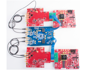
Figure 1 shows the block diagram for the setup of the TIDA-01021 clocking board for skew measurement. The connection configuration as shown in Figure 3 is as follows:

- Power:
- Power supply connector J25: This connector is used to connect the power supply. Set the power supply to 5 V with a 2-A current limit.
- Input signals:
- Option 1: The onboard VCXO Y1 is powered on using the jumper J8 and outputs a 100-MHz signal to the LMK04828 OSCin* pin input. While using Y1, disconnect the clock inputs from LMK61E2 (U2) and external reference by removing R36 and R38. At the same time, isolate the power supply to U2 by removing the jumper J16.
- Option 2: The onboard reference LMK61E2 (U2) is powered on using the jumper J16 and factory programmed to generate a 100-MHz LVDS output. U2 can be programmed to generate different clock frequencies using the I2C interface. While using U2, disconnect the clock inputs from Y1 and external reference by removing C179, R37, and R39 then place R36 and R38. Isolate the power supply to Y1 by removing the J8.
- Option 3: Connect the external reference to external OSCinP and OSCinN connectors. While connecting external reference, disconnect the Y1 and U2 connection by removing C179, R45, and R46 and place R36 and R38. Disconnect the power supply of Y1 and U2 by removing jumpers J8 and J16.
- Output signals:
- RFoutAP1, RFoutAM1, RFoutAP2, and RFoutAM2 connectors generate the DCLK and are connected to the phase noise analyzer to measure phase noise and are connected to ADC EVMs for to measure SNR.
- RFoutBP1, RFoutBM1, RFoutBP2, and RFoutBM2 connectors generate the low-frequency SYSREF signals.
- Connectors J2 and J5 generates the FPGA CLKs and SYSREFs for both channels.
- Programming interface:
- Connect the USB mini cable to the onboard USB connector U7 and test PC to program the clocking board devices using the High-Speed Data Converter (HSDC) Pro Software GUI.
2.1.2 FMC+ to FMC Adapter Board Setup
The FMC+ to FMC adapter board has connections to take FPGA clocks from the TIDA-01021 clocking or ADC12DJ3200 EVM. Follow the schematic to connect the FPGA clocks and SYSREFs from the clocking board.
2.1.3 ADC12DJ3200 EVM Setup
Follow the ADC12DJ3200 EVM user’s guide for the ADC12DJ3200 EVM hardware setup procedure.
The ADC12DJ3200 EVM has both internal as well as external options for clocking the ADC. Selecting the DEVCLK is based on the placement of capacitors on the shared pads. Connect C49 and C50 for the external DEVCLK. Connect the external SYSREF for the ADC at connector J38 from the TIDA-01021 clocking board.
2.1.4 TSW14J56 Setup
Follow the TSW14J56 EVM user’s guide for TSW14J56 EVM hardware setup procedure.
1.1 Software
1.1.1 Clocking Board Programming
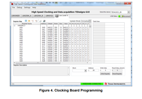
- Clocking board devices are programmed by HSDC TID GUI, as shown in Figure 4.
- All devices are configured by loading the configuration files in low-level view page.
- To measure phase noise, configure the following:
- The LMK61E2 is programmed at 100 MHz. Configure the file in low-level view page.
- The LMK04828 is taking a reference from the LMK61E2 and generates a reference to the LMX2594 through the OSCout pin. Load the config file for OSCout enable.
- The LMX2594 is programmed for a 100-MHz reference and 200-MHz phase detector frequency at various frequencies to measure the phase noise.
- To measure clock skew, configure the following:
- The LMK61E2 is programmed at 100 MHz. Configure the file in low-level view page.
- The LMK04828 is programmed in 0-dalay PLL mode at a 25-MHz SYSREF frequency and provides the SYSREFREQ and SYNC signals along with this 100-MHz OSCout as reference to both LMX2594 devices.
- Both LMX2594 devices are programmed with the common configuration file at a 25-MHz phase detector frequency and generate a 3-GHz RFoutA and 25-MHz SYSREFout (RFoutB) from both devices.
- To measure the ADC12DJ3200 SNR, configure the following:
- The LMK61E2 is programmed at 33.75 MHz. Configure the file in low-level view page.
- The LMK04828 is programmed in 0-dalay PLL mode at a 33.75-MHz SYSREF frequency and provides the SYSREFREQ and SYNC signals along with this 33.75-MHz OSCout as a reference to the LMX2594. The LMK04828 also generates the device clock and SYSREF for FPGA capture card.
- The LMX2594_A is programmed for a 2.7-GHz RFoutA and 33.75-MHz SYSREF at a 33.75- MHz phase detector frequency.
1.1.2 ADC12DJ3200 EVM Programming
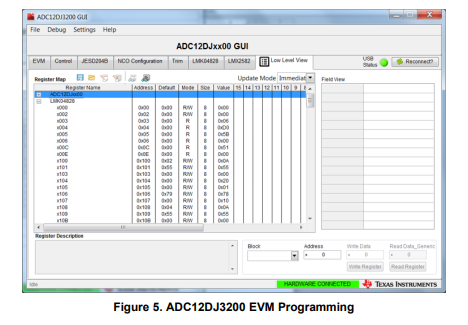
Download the ADC12DJxx00 GUI from TI.com to program the ADC12DJ3200 EVM:
http://www.ti.com/lit/zip/slac745. The ADC12DJ3200 and LMK04828 are devices configured for SNR measurement in the ADC12DJ3200 EVM, as shown in Figure 5. The LMK04828 is programmed in distribution mode for the CLKin0 drive to configure SYSREF directly. The ADC12DJ3200 EVM is put into JMODE2 mode to use in dual channel mode at full Nyquist zone of the device. The EVM is setup in external clock source selection mode, with a sampling frequency 2700 Msps and load configuration files in the low-level view page of the ADC12DJ3200 GUI.
1.1.3 HSDC Pro Setup
The HSDC Pro software interfaces with the TSW14J56 to capture and analyze the digital data from the ADC12DJ3200 in SNR measurement. Follow the TSW14J56 EVM user’s guide for HSDC Pro setup and to capture and analyze the data.
2 Testing and Results
2.1 Test Setup
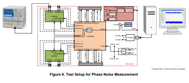
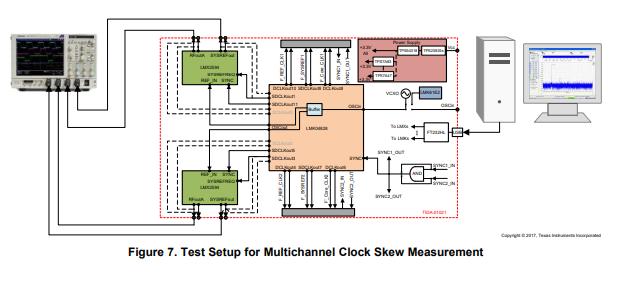
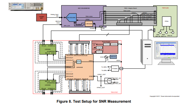
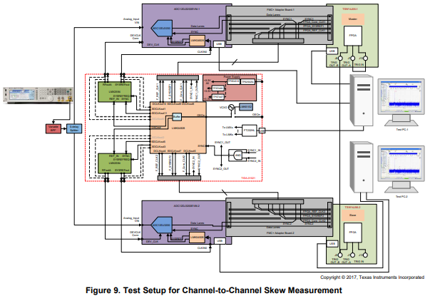
Figure 6, Figure 7, Figure 8, and Figure 9 show the test setup for LMX2594 phase noise, clock skew, SNR measurement, and channel-to-channel skew measurement, respectively.
2.2 Results
2.2.1 Phase Noise Performance
Both LMX2594 devices show almost the same results as both are identical on board. Measured phase noise plots are shown in Figure 10, Figure 11, and Figure 12.
 2.2.2 Multichannel Clock Phase Alignment
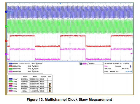
As explained in Section 2.3.2, synchronized clocks are critical for multichannel systems. This section shows the measured phase aligned clocks and SYSREFs that are generated from both LMX2594 devices at a 3-GHz device clock and 25-MHz SYSREF. The minimum skew have between the clocks, reflects the minimum channel-to-channel skew in multichannel systems. In this test, the TIDA-01021 clock board shows the clock skew less than 10 ps. As a result, it can reduce the channel-to-channel skew in multichannel systems. Figure 13 shows the multichannel clock skew measured results from two LMX2594 devices at the device clocks and SYSREF signals.
2.2.3 Signal Chain Performance
The comparison between the measured SNR with the ADC12DJ3200EVM onboard clocks and with TIDA-01021 clocks shows slight difference in SNR due to a lower PFD frequency in used in the TIDA-01021 clock synthesizer (LMX2594). The lower PFD frequency was selected to allow multichannel synchronized DEVCLK and SYSREF generation. Figure 14, Figure 15, and Figure 16 shows the spectral results at a 2700-MHz sampling frequency in dual-channel mode.
 1.1.1 Channel-to-Channel Skew Measurement
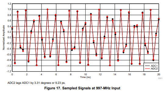
This skew is evaluated by calculating the phase difference between signals captured from each ADC. These measurements taken at a 2.7-GHz sampling frequency and measured time skew was < 50 ps for each input frequencies.
Figure 17 is a plot of the output samples of the two ADCs for a 997-MHz input, which is in first Nyquist zone for a 2700-MHz sampling clock. Figure 18 is the plot of the output samples for a 2482-MHz input, which is in second Nyquist zone for a 2700-MHz sampling clock. The 2482-MHz input signal aliases to 218 MHz and a phase difference of 8.35 degrees is measured, which translates to a channel-to-channel skew of 9.35 ps for the 2482-MHz input.

1.2 Summary and Conclusion
The TIDA-01021 design is a multichannel JESD204B compliant clocking reference design that can be used for DSO, radar, and 5G wireless testers. This TI Design demonstrates a high-performance (lowphase noise) clock generation, using the LMX2594, LMK61E2 and LMK04828 devices. This design also demonstrates the multichannel configurable phase synchronized clocks with skew of less than 10 ps. Finally, the ADC12DJ3200 EVM onboard clock is replaced with TIDA-01021 outputs to demonstrate the impact on system performance. The system SNR is close to the ADC12DJ3200EVM performance and clock skew at less than 10 ps. The system shows deterministic latency behavior for every power ON cycle with the analog input channel-to-channel skew at less than 50 ps.
For more information, visit: Texas Instruments