


 platforms. By providing a configuration that emulates common voltage rails and peripherals, this design can be used as a reference design across multiple TV power)
Description
The TIDA-050027 reference design is a power distribution solution for television (TV) platforms. By providing a configuration that emulates common voltage rails and peripherals, this design can be used as a reference design across multiple TV power architecture including LCD and OLED TV. On the input, an eFuse is used for short-circuit protection, while the high-efficiency buck converters provide the necessary power for the core rail, always-on rails, and peripheral rails. Additionally, low IQ low-dropout regulators (LDOs) provide clean digital-power for certain peripheral rails. In addition to these power components, load switches control the voltage with controlled slew rates to allow for power sequencing and power savings. Additionally, integrated load switches provide self protection while reducing bill of materials (BOM) count and solution size.


 Features
- Fully-featured power tree for common TV rails allow for appropriate selection of load switches, buck converters, and LDOs in system design
- High-efficiency buck converters with fast transient response and reduced Bill of Material (BOM) count for smaller solution size
- Integrated protection features improves system reliability and reduces customer returns
- Switching OFF unused loads results in higher system efficiency and lower standby current
- Load switches offer smaller solution size and lower component count when compared to discrete FET solutions.
Applications
- HDTV
- UHD 4K OLED TV
- UHD LCD TV
 1 System Description
This reference design showcases a power distribution solution for televisions (TVs). Since many TV architectures require similar core voltage and peripheral rails, this design can be used across multiple TV architectures including OLED and LCD TVs.
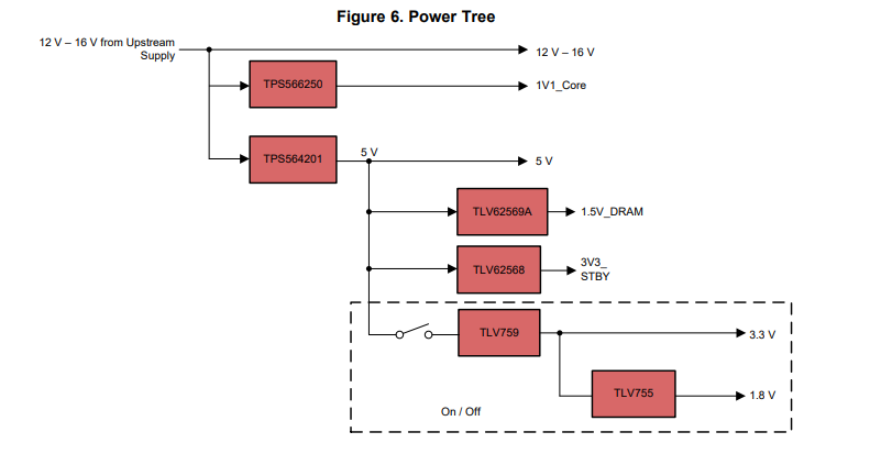
This design incorporates four buck converters as well as two LDOs to power the core rails, always-on rails, memory, and peripherals such as USB ports and TV tuner. Each buck converter is chosen to handle specific requirements for each of the rails. For the core rail, the requirements include steady output voltage with very good transient response to avoid affecting performance. The remainder of the rails require high efficiency with good transient response. The LDOs for the peripherals provide a IQ power supply that also require a clean-power supply such as the TV Tuner.
This design also incorporates nine load switches for peripheral loads commonly found on most TVs including: Panel Power (TCON), Stand-by (STBY) rails, WIFI, NAND, USB, and TV Tuner blocks. All of the load switches have their ON pins connected to external jumpers for quick access to each peripheral rail. An eFuse at the input manages short-circuit and overvoltage events that could potentially damage downstream DC/DC converters and load switches. The reference design also includes common voltage rails found in most TV solutions, including 5 V Peripheral, 3.3 V Standby, 1.5 V DRAM, 3.3 V I/O, and 1.1 V Core rail. Finally, a USB-A header is included at the output of the 5 V USB switch to support USB loads. By using integrated devices, this reference design reduces BOM count, improves system reliability, and enables faster design cycles.
Each main voltage rail (5 V, 3.3 V, and 1.8 V) is accompanied by a discrete FET solution. This allows a direct performance comparison between the integrated load switch and a discrete FET solution. Test points are included at the output of each peripheral and voltage rail, and silkscreen traces outline the size of each solution.
| 1.1 Key System Specifications | |||||||||
| Table 1. Key System Specifications | |||||||||
| PARAMETER | SPECIFICATIONS | DETAILS | |||||||
| Input voltage range | VIN | 12 V to 16 V | |||||||
| DEVICES | DEVICES | VIN | VOUT | IOUT | |||||
| DC/DCS | TPS564201 | 12 V to 16 V | 5 V | 4 A | |||||
| TPS566250 | 12 V to 16 V | 1 V | 6 A | ||||||
| TLV62569A | 5 V | 1.5 V | 2 A | ||||||
| TLV62568 | 5 V | 3.3 V | 1 A | ||||||
| LDOs | TLV759P | 5 V | 1.8 V | 1 A | |||||
| TLV75518 | 3.3 V | 1.8 V | 400 mA | ||||||
| PARAMETER | DEVICES | VIN | RON | IOUT | |||||
| eFuse | TPS2595 | 12 V to 16 V | 34 mΩ | 4 A | |||||
| Load Switch | TPS22810 | 12 V to 16 V | 79 mΩ | 2 A | |||||
| TPS22975 | 5 V | 16 mΩ | 6 A | ||||||
| TPS22919 | 5 V, 3.3 V, 1.8 V | 89 mΩ at 5 V | 1.5 A | ||||||
| USB Switch | TPS25221 | 5 V | 70 mΩ | 2 A | |||||
2 System Overview
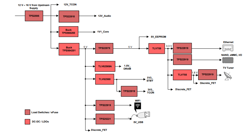
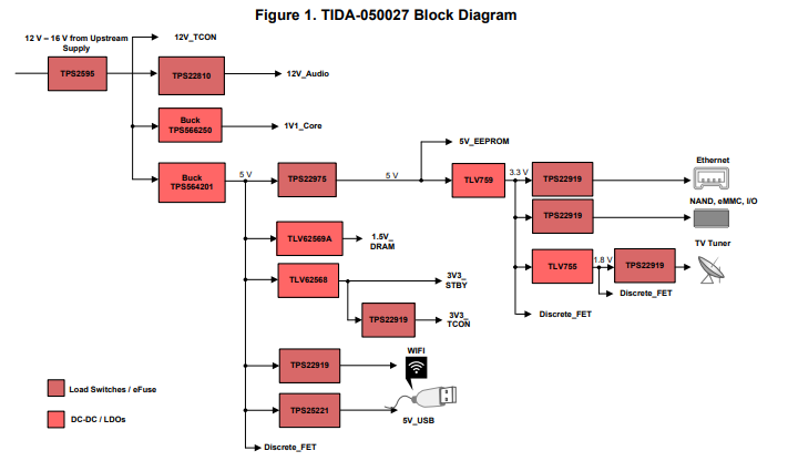
2.1 Block Diagram
 2.2 Design Considerations
2.2.1 Total Solution Size
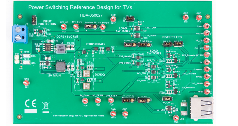
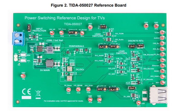
Referring to Figure 2, the design is laid out in three main stages: Front-end stage, Power Stage, and Peripherals. Using integrated devices simplifies the solution complexity while keeping the PCB space as compact and space-efficient as possible.
 The front-end stage includes an eFuse at the input alongside two DC/DCs. The TPS2595 eFuse provides short-circuit and overvoltage protection, while the two DC/DCs emulate voltage rails commonly found on televisions: a 1.1 V core (1V1_CORE) and a 5 V rail for downstream components. The core rail is an always-on, high current rail for the TV SoC, while the 5 V rail leads to downstream power components. The total solution size of the front end components is 111mm2, with 7mm2 for the eFuse and 104mm2 for the DC/DC components.
The power stage components consist of additional DC/DCs to power a 3.3 V standby rail (3V3_STBY), as well as a 1.5 V rail for DRAM or SoC Memory modules. The standby rail is useful when the TV enters a low-power mode, such as a sleep or rest state. The 1.5 V rail is another high current rail used for additional SoC modules, such a memory or DRAM. The total solution size of the DC/DC components is 56mm2. There are also 5 V peripherals connected to the 5 V rail with integrated load switches, including WiFi (5V_WIFI) and USB (5V_USB). A discrete FET implementation is also included to compare performance and size against an integrated solution.
The Peripherals included on this TV reference design emulate common rails and outputs found on TV power designs. A TPS22975 load switch is included at the input of the 5 V peripheral rail, allowing easy access to power down all of the peripherals, for example during standby mode. An LDO converts the 5 V rail into a 3.3 V rail for peripherals including Ethernet, NAND, eMMC, and I/O. Another LDO branches off the 3.3 V down to 1.8 V, providing access to 1.8 V loads such as TV tuners and digital voltage rails required by the SoC. Finally, load switches are included on the front end 12 V line for 12 V rails such as audio and TCON.
Table 2. Solution Area Size
| Name of Box | Included Components | Total Solution Size |
| Input Protection | TPS2595 | 7mm2 |
| Core / SoC Rail | TPS566250 | 57mm2 |
| 5 V Main | TPS564201 | 47mm2 |
| DC/DCs | TLV62568, TLV62569A | 56mm2 |
| Peripherals | TPS22975, TLV757 | 14.18mm2 |
2.2.2 Power Switching Complexity and Size
As televisions push for higher resolution and greater complexity, their power designs are also getting larger and more complex. As the number of power rails and peripherals increases, additional devices and passive components need to be selected and integrated into the system. As the BOM complexity increases, the number of design considerations increase: including design and layout cycles, PCB space, and points of failure/visual inspection.
A discrete switching circuit contains several components to control the turnon and turnoff behavior of a discrete power MOSFET. Figure 3 shows a common discrete FET implementation, which is used on the reference design. In comparison, Figure 4 shows a TPS22919 integrated load switch that can also be used to turn on and or off the corresponding load. Compared to a discrete solution, integrated load switches reduce the BOM count, which helps to reduce the total solution complexity and size.
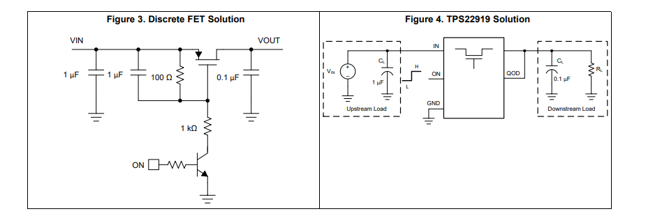 Features such as self-protection and recovery from short circuits, controlled slew rate, thermal shutdown, and quick output discharge (QOD), would require additional components or oversized FETs to be done discretely. With an integrated load switch, this can be accomplished using a single device. Section 3.2.2 will demonstrate and compare the discrete circuit and the TPS22919 in-depth, providing power on and or off waveforms, thermal images, and transient event waveforms. For more information regarding the drawbacks and limitations of a discrete switching solution, please refer to Integrated Load Switches versus Discrete MOSFETs app note.
Table 3. Discrete FET vs.TPS22919 Load Switch Comparison
| Discrete Solution | TPS22919 | |
| BOM Count | 6 components | 1 component |
| Solution Size | 17.08mm2 | 4.1mm2 |
| Rise Time | RC Based | Linear, ~1 ms |
| Thermal Shutdown | ✓ | |
| Short Circuit Protection | ✓ | |
| Quick Output Discharge (QOD) | Implemented using External Components | ✓ |
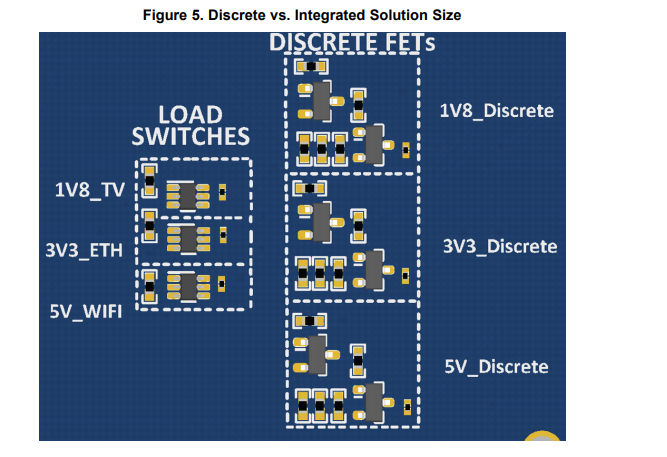
Figure 5 compares the solution size of both switching solutions. The three discrete FETs, (1 V8_DIS, 3V3_DIS, 5V_DIS), consists of 18 components with a total solution size of 275mm2. In comparison, the three integrated rails consists of three TPS22919 load switches, with a 76 percent reduction in solution size.
Copyright © 2019, Texas Instruments Incorporated
Table 4. Discrete vs. Integrated Solution Size
| Solution | Included Components | Number of Components | Total Solution Size |
| 3 Load Switches | 3* TPS22919 (1V8_TV, 3V3_ETH, 5V_WIFI) | 3 | 12.3mm2 |
| 3 Discrete FETs | 3* PMOS FET
3* BJT 9 *Resistors 3*Gate Capacitor |
18 | 51.24 mm 2 |
Figure 5. Discrete vs. Integrated Solution Size
 2.2.3 Protection Features
Protection features allows for safer and more reliable systems, reducing system failures and customer returns. In television power architectures, features such as inrush current protection, short circuit protection, thermal shutdown, and power sequencing ensure that the system remains robust, while preventing damage to sensitive components.
During startup, inrush current is controlled to protect the MOSFET, PCB traces, and prevent voltage dip that could leave the system in an undesired state. When power is initially applied to the system, capacitor charging can result in a spike of inrush current, which can exceed the nominal load current. The TPS2595 eFuse at the input manages inrush current to the downstream voltage rails, while the TPS22919 manages inrush current to the various peripheral loads. By increasing the rise time of each voltage rail using slew rate control, this minimizes the inrush current while protecting the downstream load. To implement this configuration using discrete components, additional passive components such as a gate resistor and capacitors need to be included, which increases BOM count, solution size, and timing complexity.
The eFuse and integrated load switches also provide short circuit protection and thermal shutdown. The eFuse at the input prevents damage to downstream components in case of an overvoltage/overcurrent or fault condition, while the TPS22919 offers self protection, meaning that it will protect itself from short circuit events on the peripheral rails. The TPS22919 also has thermal shutdown to prevent damage to the device from overheating, which could occur during startup into a capacitive load or a high-current fault condition.
2.2.4 Power Consumption
To reduce standby power for the system, this reference design reduces power consumption by choosing high efficiency and low IQ power components and by disconnecting loads and peripherals from DC/DC converters when not in use, which is common practice in standby mode.
In this design, load switches are used to emulate various peripheral rails, which can be turned on or off when not in use. If the TV requires all the peripherals to be off in a certain mode, such as standby mode, the TPS22975 can also be used to turn off all the various peripheral rails. The switches can also be used for power sequencing. Power Sequencing is critical for voltage rails that must turn on in a specific order to ensure operation safety and reliability. Sequencing the rails also staggers the inrush current during startup, which reduces system stress and prevents unexpected reverse bias conditions. On this TV power design, the load switches can be sequenced to ensure that the core rails (1V1_CORE, DRAM, Panel), are up before the peripheral rails are operational.
Televisions also contain always-on rails to power critical system components such as core SoC rails, standby rails, and DRAM power. These rails must remain on throughout all operation modes. Therefore, all of the four DC/DC converters remain enabled to emulate powering always-on loads.
 2.3 Highlighted Products
2.3.1 TPS22919
The TPS22919 device is a small, single channel load switch with controlled slew rate. When power is first applied, a Smart Pull Down is used to keep the ON pin from floating until system sequencing is complete. When the pin is deliberately driven High (>VIH), the Smart Pull Down is disconnected to prevent unnecessary power loss. The TPS22919 load switch is also self-protected, meaning that it will protect itself from short circuit events on the output of the device. It also has thermal shutdown to prevent any damage from overheating.
2.3.2 TPS22810
The TPS22810 is a single channel load switch with configurable rise time and with an integrated quick output discharge (QOD). In addition, the device features thermal shutdown to protect the device against high junction temperature. Because of this, safe operating area of the device is inherently ensured. The device contains an N-channel MOSFET that can operate over an input voltage range of 2.7 V to 18 V.
2.3.3 TPS22975
The TPS22975 is a single-channel load switch that provides a configurable rise time to minimize inrush current. TPS22975 has an optional 230-Ω on-chip load resistor for quick output discharge when switch is turned off. The TPS22975 is available in a small, space-saving 2-mm × 2-mm 8-pin SON package ( DSG ) with integrated thermal pad allowing for high power dissipation.
2.3.4 TPS2595
The TPS2595 eFuse (integrated FET hot swap devices) is a highly integrated circuit protection and power management solution in a small package. The device provides multiple protection modes using very few external components and are a robust defense against overloads, short circuits, voltage surges, and excessive inrush current.
2.3.5 TPS566260
The TPS566250 is a 18 V, 6A synchronous step-down (buck) converter with dynamic voltage scaling (DVS) capability through I2c . It operates using D-CAP2™ control mode which provides very fast transient response, and reduces the required output capacitance required to meet a specific level of performance. This device also would not require external compensation which reduces the total size and cost of implementation. The output voltage of the device can be set by either FB with resistor divider or it can be dynamically set from 0.6 V ~ 1.87 V through I2C compatible interface.
2.3.6 TPS564201A
The TPS564201 is a simple, easy-to-use, 4-A synchronous step-down converter in SOT-23 package. The device is optimized to operate with minimum external component count and also optimized to achieve high efficiency at both normal and light load conditions. This solution is a part of a pin-to-pin compatible family of devices ( TPS56x201 ) which would support from 1A ~5A current loads.
2.3.7 TLV65268
The TLV62568 device is a synchronous step-down buck DC-DC converter optimized for high efficiency and compact solution size. The device integrates switches capable of delivering an output current up to 1A. In order to provide the lowest power consumption for an always on rail, the device enters power save mode at light loads. If lower ripple is required, the TLV62568A can be used instead. In shutdown, the current consumption is reduced to less than 2 μA.
2.3.8 TLV65269A
The TLV62569A device is a synchronous step-down buck DC-DC converter optimized for high efficiency and compact solution size. The device integrates switches capable of delivering an output current up to 2 A. In order to provide the lowest ripple and best transient response for powering the DRAM rail, the device operates only in pulse width modulation (PWM) mode without a power saving mode. If light load efficiency is important, the TLV62569 can be used instead. In shutdown, the current consumption is reduced to less than 2 μA.
2.3.9 TLV755/7P
The TLV755P is an ultra-small, low quiescent current, low-dropout regulator (LDO) that sources 500 mA and 1 A for the TLV757P, with good line and load transient performance. The TLV755P is optimized for a wider variety of applications by supporting an input voltage range from 1.45 V to 5.5 V. To minimize cost and solution size, the device is offered in fixed output voltages ranging from 0.6 V to 5 V to support the lower core voltages of modern microcontrollers (MCUs). Additionally, the TLV755P has a low IQ with enable functionality to minimize stand-by power. When shutdown, the device actively pulls down the output to quickly discharge the outputs and ensure a known start-up state.
2.3.10 TLV758/9P
The TLV759P low-dropout regulator (LDO) is an adjustable output, ultra-small, low quiescent current LDO that sources 1 A and 500mA for the TLV758P, with good line and load transient performance. The TLV759P is optimized for a wide variety of applications by supporting an input voltage range from 1.45 V to 5.5 V. Additionally, the TLV759P has a low IQ with enable functionality to minimize standby power. When shutdown, the device actively pulls down the output to quickly discharge the outputs and ensure a known start-up state. Furthermore, the TLV759P supports adjustable output via resistor divider for voltage options not supported by the TLV755/7.
3 Hardware, Software, Testing Requirements, and Test Results
3.1 Required Hardware
3.1.1 System Overview
The TIDA-050027 TV Reference Design power rails can be sequenced depending on the downstream loads and peripherals. Table 5 provides an overview of the jumpers and test points on the TI Design.
Table 5. Jumper/Connector Summary
| Stage | Connector | Label | Description |
| Input | J2 | – | Input Power, connector for 12 16 V |
| JP9 | – | Enable for TPS2595 (U12) | |
| TP21 | 12V_UP | Test Point for eFuse output | |
| CORE / SoC Rail | JP11, TP23, TP24 | SDA / SCL | Test Points for TPS566250 communication |
| TP22 | 1V1_Core | Test Point for DC/DC output | |
| 5 V Main | TP25 | 5V_Down | Test Point for DC/DC output |
| DC/DCs | TP19 | 1V5_DRAM | Test Point for DC/DC output |
| TP20 | 3V3_STBY | Test Point for DC/DC output | |
| Peripherals | JP5 | Peripheral_EN | Enable for TPS22975 |
| TP14 | 5V_Periph | Output of 5 V Peripheral Rail | |
| Load Switches | JP10 | 12V_EN | Enable for TPS22810 |
| JP2 | 3V3_EN | Enable for TPS22919 | |
| JP1 | 1V8_EN | Enable for TPS22919 | |
| JP7 | 5V_EN | Enable for TPS22919 | |
| TP8 | TV | Output of 1.8 V Peripheral Rail | |
| TP1 | TCON | Output 12 V Rail | |
| TP4 | Audio | Output 12 V Rail | |
| TP9 | Ethernet | Output of 3.3 V Peripheral Rail | |
| TP10 | NAND | Output of 3.3 V Peripheral Rail | |
| TP11 | 3V3_Panel | Output of 3.3 V Standby Rail | |
| TP12 | WIFI | Output of 5 V Peripheral Rail | |
| Discrete FETs | JP3 | 1V8_D_EN | Enable for Discrete FET |
| JP4 | 3V3_D_EN | Enable for Discrete FET | |
| JP8 | 5V_D_EN | Enable for Discrete FET | |
| TP5 | 1V8_Dis | Output of 1.8 V Discrete Rail | |
| TP6 | 3V3_Dis | Output of 3.3 V Discrete Rail | |
| TP7 | 5V_Dis | Output of 5 V Discrete Rail |
3.2 Testing and Results
3.2.1 Test Setup
To configure the reference design for operation, connect the jumpers as shown in Figure 7.
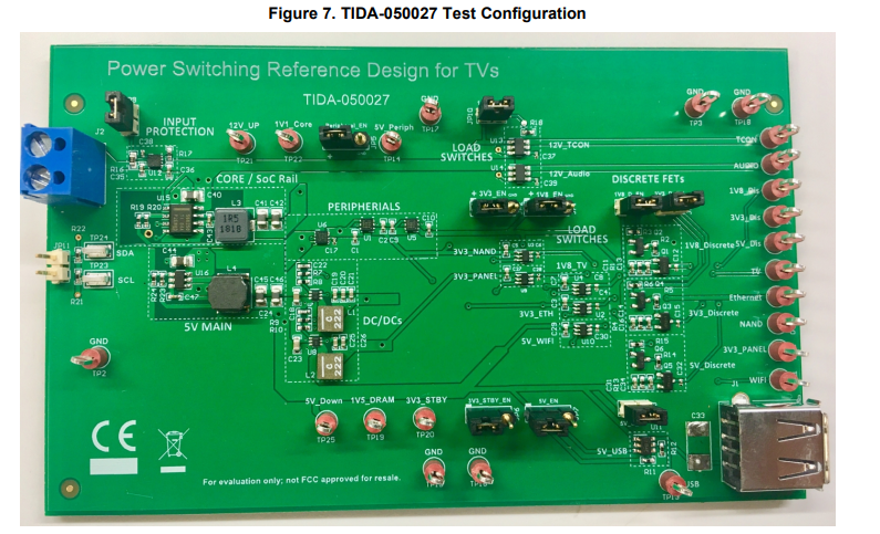 Table 6. TV Configuration Setup
| Description | Jumper / Connector | Value |
| Input Power, connector for 12 16 V | J2 | Connect pins 1 and 2 |
| 12 V Load Switch enable | JP5, JP10 | Connect pins 1 and 2 |
| 5 V, 3.3 V, 1.8 V Load Switch enable | JP1, JP2, JP6, JP7 | Connect pins 1 and 2 |
| Discrete FET Enable | JP3, JP4, JP8 | Connect pins 1 and 2 |
3.2.2 Test Results
3.2.2.1 Power Sequencing Demonstration
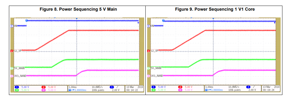
Power Sequencing is critical on voltage rails that must turn on in a specific order to ensure operational safety and reliability. For example, core rails for downstream SoCs and microcontrollers need to be powered before WIFI and other peripherals are turned on. Sequencing the rails also helps stagger the inrush current during power-up, which reduces system stress and prevents unexpected reverse bias conditions.
The TV Reference Design’s voltage rails are sequenced to emulate the power-on of a television system. After the system is initially turned on, the 12 -16 V input passes downstream and turns on the two critical rails, 1V1_Core and 5 V Main. Once both of these rails are high, the 5 V Peripherals are turned on followed by the 3.3 V and 1.8 V Peripherals. Figure 8 and Figure 9 demonstrate the power-on sequence.
 3.2.2.2 Standby Power Demonstration
The system standby current measurements were taken in various on/off modes. In standby mode, the measured input current was 1.256mA. This includes all of the necessary “always-on” core rails, including 1V1_Core and 3V3_STBY. With all of the peripherals and load switches enabled, the design was drawing roughly 1.5mA of quiescent current. This accounts for all of the LDOs and peripheral load switches, which drew an additional 220 μA current when enabled. In comparison, three discrete FETs drew roughly 500μA when enabled.
Table 7. Measured Input Current
| Mode of Operation | Devices Enabled | Measured Input Current |
| Standby Mode | TPS2595, TPS566250, TPS564201, TLV62569A, TLV62568 | 1.256 mA |
| Everything on except Discrete FETs | TPS2595, TPS566250, TPS564201, TLV62569A, TLV62568,
TPS22975, TLV757, TPS22919 |
1.478 mA |
| All Devices Enabled | TPS2595, TPS566250, TPS564201, TLV62569A, TLV62568, TPS22975, TLV757, TPS22919, 1V8_Dis, 3V3_Dis, 5 V_Dis | 1.923 mA |
3.2.2.3 Discrete FET vs. Integrated Load Switch Comparison
Table 8. Turn On/Off Summary Table
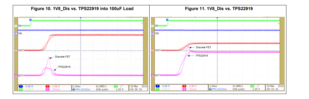
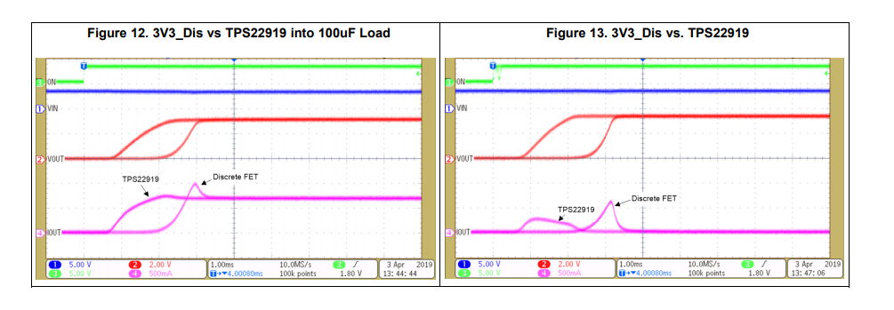
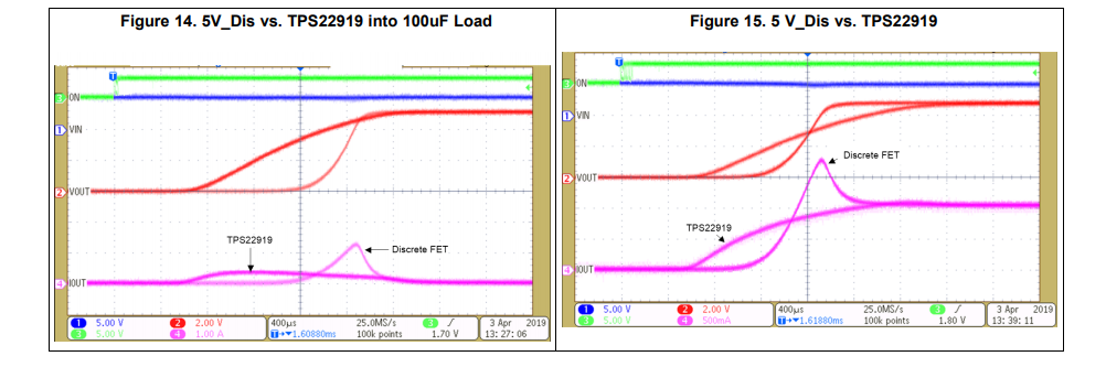
| Voltage | Parameter | Description | Section |
| 1.8 V | 1.8 V Capacitive Load | 100uF | Figure 10 |
| 1.8 V Load | 100uF, 3.6Ω (500mA) | Figure 11 | |
| 3.3 V | 3.3 V Capacitive Load | 100uF | Figure 12 |
| 3.3 V Load | 100uF, 5.5Ω (600mA) | Figure 13 | |
| 5 V | 5 V Capacitive Load | 100uF | Figure 14 |
| 5 V Load | 100uF, 1Ω (1A) | Figure 15 |
3.2.2.3.1 1.8V Load Demonstration
As shown in Figure 4 the discrete solution contains an NPN BJT is connected to the gate of the PMOS “pass FET.” When the NPN BJT is enabled, it pulls down the gate of the PMOS and allows for power to flow from VIN to VOUT. However, compared to a TPS22919 solution, the discrete solution comes with a set of limitations. During power on and or off sequences, the discrete solution will have a nonlinear ( RC ) turn-on behavior, which can lead to a large spike of inrush current. The following waveforms will compare/contrast the turnon behaviors overlaid on one another. In the first waveform, Figure 10, both switching solutions are starting into a 100uF capacitive load. The TPS22919 exhibits a linear turn on behavior, limiting the inrush current to roughly 200mA. In comparison, the discrete solution experiences a peak of over 400mA of inrush current. In Figure 11, both solutions are starting into a 500mA / 100uF load. The TPS22919 helps to manage the inrush current with the controlled slew rate, while the discrete solution peaks at 700mA of inrush current.
 3.2.2.3.2 3.3V Load Demonstration
Figure 12 and Figure 13 provide a comparison between the discrete solution and the TPS22919 at 3.3 V. When starting into a capacitive load, the TPS22919 limits the inrush current to 250mA while the inrush current on the discrete solution jumps to 700mA. When starting into a 1A load with 100uF of capacitance, the TPS22919 limits the inrush current while the discrete FET peaks to 1 A.
 3.2.2.3.3 5 V Load Demonstration
Figure 14 and Figure 15 provide a comparison between the discrete solution and the TPS22919 at 5 V. When starting into a capacitive load, the TPS22919 limits the inrush current to 250mA while the inrush current on the discrete solution jumps to 1.3A. When starting into a 1A load with 100uF of capacitance, the TPS22919 limits the inrush current while the discrete FET peaks at over 1.75 A.
 3.2.2.3.4 Thermal Protection
Thermal shutdown protects the device from failure when the device junction temperature exceeds its safe limit. During operation, the junction temperature can rise due to many factors, including a high current load, large inrush current during startup, or during a fault condition. Thermal protection turns off the switch to protect itself by reducing the power dissipation, also potentially avoiding damage to upstream and downstream components. In comparison, a discrete FET cannot protect itself if it exceeds it’s thermal junction temperature. In this case, the FET could potentially break, causing a short and damaging the downstream load or peripheral.
Figure 16 and Figure 17 provide a thermal image of the TPS22919 with a high current load at 25C. In this scenario, a 3A load is connected to 3V3_Eth, causing the thermal junction temperature to rise. As the temperature increases past 144C, the TPS22919 turns off and thermal cycles, bringing the board temperature back down to roughly 85 C.
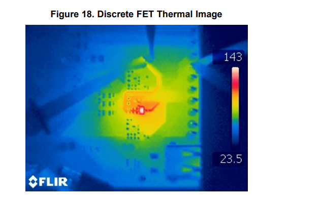
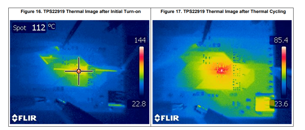 In comparison, Figure 18 shows the package temperature of the discrete FET at 25C under the same 3 A load. The 3.3 V discrete FET will continue to power the downstream load until it fails. Unlike the TPS22919, the discrete FET does not have thermal shutdown, and will continue to be thermally stressed until the load is removed. If the FET is stressed beyond its absolute maximum rating, the device could also potentially be damaged. At higher ambient temperatures, the discrete FET will continue to be stressed beyond 143C, whereas the TPS22919 will continue to protect itself and thermally cycle.
 3.2.2.3.5 Transient Protection Features
TV Power Architectures can be stressed during startup and fault conditions. During these conditions, discrete FETs can dissipate more power that exceeds the physical and thermal limits of the MOSFET. If proper tests aren’t taken into consideration, the system can fail due to overstressing these components. Additionally, some of these fault conditions, such as short circuit protection and hot plug protection, are often difficult to implement discretely and require additional components and design complexity. By using integrated devices on the TIDA-050027, these additional protection features can make the design more robust while simplifying the design.
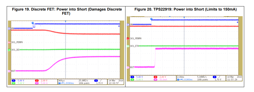
The first major transient event that could severely damage the system is Power Into Short. In this condition, the output of the FET / IC is shorted to ground before the switch is turned on. As the FET is turned on, VOUT remains grounded at 0V. Therefore, the stress across the FET is equal to VIN. The power dissipated into the FET is equal to VIN * IOUT. Done discretely, as shown in Figure 19, the FET doesn’t limit the current in the transient event and passes 10A of current downstream. Since the junction temperature of the FET exceeds its thermal limit during this event, the FET is damaged and sends 10A of continuous current to the downstream component.
In comparison, the TPS22919 integrated load switch is self-protecting and prevents damaging itself during the power into short event. When the short occurs, the large VIN to VOUT voltage drop causes the switch to limit the output current (Isc). Since the output voltage starts at 0 V, a lower limit is used to minimize the power dissipation until the fault is removed. In this case, as shown in Figure 20, the TPS22919 limits the output current to 0.5A while protecting itself from damage.
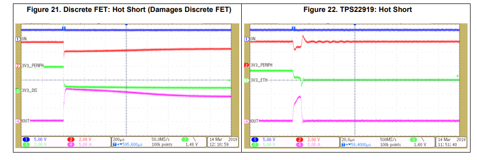
The other major transient event that could severely damage the system is Hot Short. In this condition, the output of the FET / IC is shorted to ground when the device is already turned on. This event is considered the more stressful event since the switch usually starts out hotter due to the pre-existing load current. The power dissipated into the switch is equal to VIN * IOUT. Figure 21 demonstrates a discrete implementation. Since the discrete FET doesn’t limit the current in the transient, more than 10A passes downstream and the FET fails.
In comparison, the TPS22919 integrated load switch measures the voltage drop across the device and limits the output current within tsc. The device continues to limit the current until it reaches the thermal shutdown temperature. At this point, the device turns off until the junction temperature has lowered. As shown in Figure 22 the TPS22919 limits the output current and turns off, dropping the output voltage to 0 V and protecting itself from damage.
 3.2.2.4 DC/DC Efficiency and Transient Testing Results
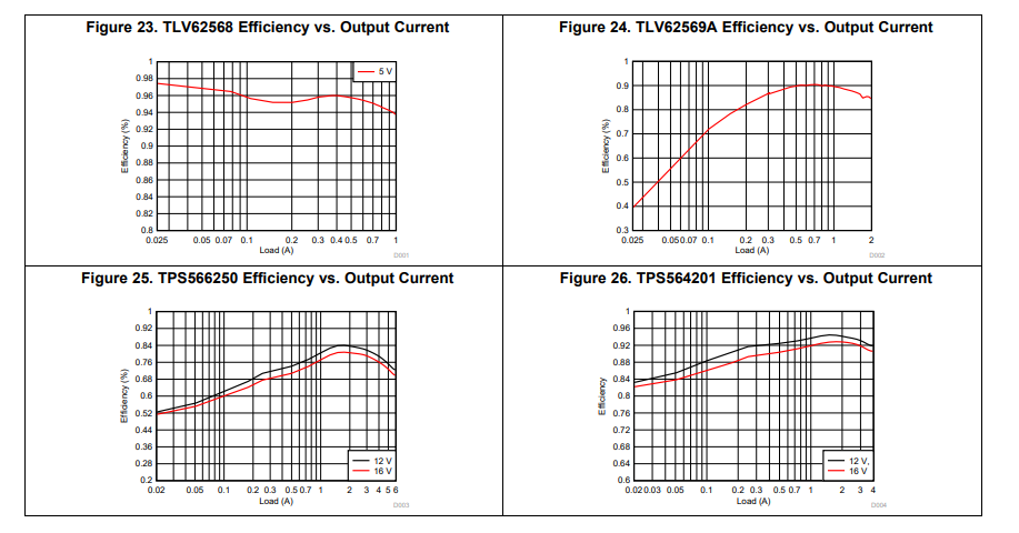
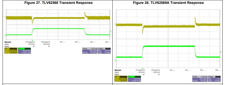
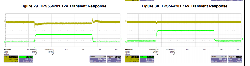
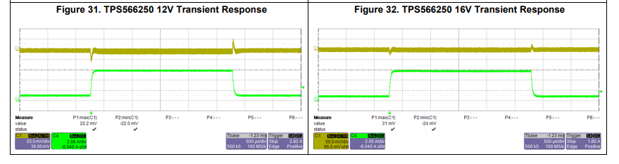
Figure 23, Figure 24, Figure 25, and Figure 26 provides the TIDA-050027 DC/DC efficiency results. Figure 27, Figure 28, Figure 29, Figure 30, Figure 31, and Figure 32 provides the TIDA-050027 DC/DC transient responses.
 Article Courtesy: Texas Instruments