Introduction to the LTC7050 SilentMOS Family
This article introduces the Analog Devices LTC7050 SilentMOS family. This new high current point of load converters satisfies the growing need for high efficiency, high density, and reliable power stage for system designs.


Why the Analog Devices LTC7050 SilentMOS Family Is the Ideal Choice
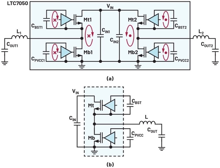
The LTC7050 can be configured to power two separate rails, with individual on/ off control, fault reporting, and current sensing outputs, or it can be configured as a dual-phase single output converter. The LTC7051 single 140 A power stage leverages the LTC7050 core design and offers even higher power density with a single inductor.
The LTC7050 dual monolithic power stage fully integrates high-speed drivers with low resistance half-bridge power switches plus comprehensive monitoring and protection circuitry in an electrically and thermally optimized package. With a suitable high-frequency controller, this power stage forms a compact, high current voltage regulator system with state-of-the-art efficiency and transient response. Silent Switcher® 2 architecture and integrated bootstrapped supplies allow high-speed switching, decreasing high-frequency power loss by attenuating input supply or switch node voltage overshoot and minimizing attendant EMI.
Low Switch Node Stress Enhances the Robustness of the Power Stage
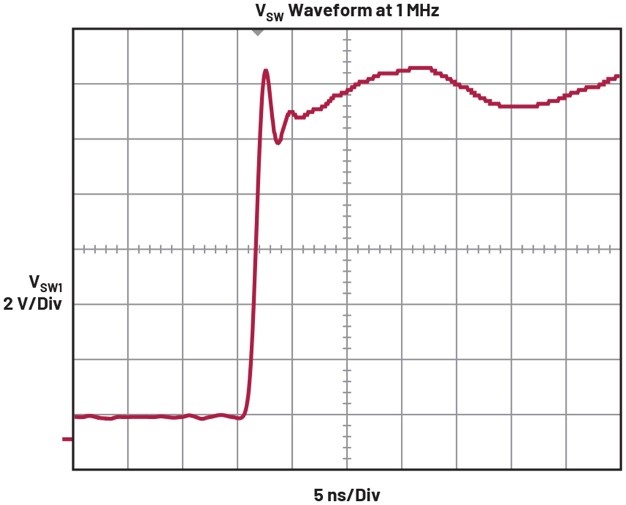
In conventional buck regulator designs, the hot loop inductance between the input capacitor and power MOSFETs leads to large spikes at the switch node. Using Silent Switcher 2 technology, the SilentMOS LTC7050 integrates critical VIN decoupling capacitors inside the LQFN package. Shrinking the hot loops results in lower parasitic inductance. In addition, the fully symmetrical layout cancels the electromagnetic fields. Figure 1 compares the LTC7050 layout with a conventional power stage. As shown in Figure 2, the peak voltage of the switch node is only 13 V when the input voltage is 12 V and output is fully loaded. The ample margin between peak voltage stress on the power MOSFET and its voltage rating ensures the reliability of the device. The fully integrated hot loops eliminate PCB layout sensitivity and make the sophisticated electromagnetic cancellation design transparent to the user. To correctly measure switch node ringing, use a coax cable soldered from the switching pin to its local ground and measure the waveform with a matched impedance at the oscilloscope.
High Efficiency and Advanced Package Enables High Power Density
Because of its low transition loss, the LTC7050 is more efficient than the conventional DrMOS module in high-frequency designs. The overlapping time of power device current and voltage is determined by the driving speed. In a multidie DrMOS module, driving speed is limited by the inductance between drivers and power MOSFETs, as well as between drivers and their capacitors. Driving MOSFET gates too quickly may lead to overvoltage at the gates of power devices/drivers and cause failure. Also, the high di/dt will cause a large spike at the switch node since the hot loop inductance is not negligible.
LTC7050’s drivers are integrated on the same die as the power stage, and the capacitors for all gate drivers are in package. With the bonding wires eliminated, the parasitic inductance in each driving loop approaches zero. Compared with a multidie DrMOS module, LTC7050 turns on and off the power devices much faster. A typical rising edge of switched node voltage is as short as 1 ns, as shown in Figure 2. Its best-in-class fast driving speed greatly reduces the transition loss. Fast driving speed permits the LTC7050 to have zero dead time, greatly reducing diode conduction and reverse recovery losses.
The sophisticated design boosts the power conversion efficiency at high switching frequencies. Figure 3 shows the 12 V to 1.8 V conversion efficiency and loss curve at 600 kHz and 1 MHz. The peak efficiency is over 94% for the 1 MHz design.
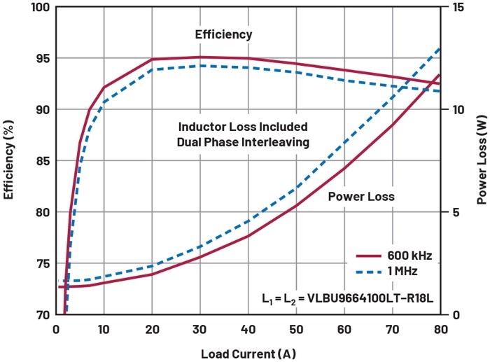
Figure 4 shows the 12 V to 1.0 V conversion efficiency and loss curve at 600 kHz and 1 MHz.
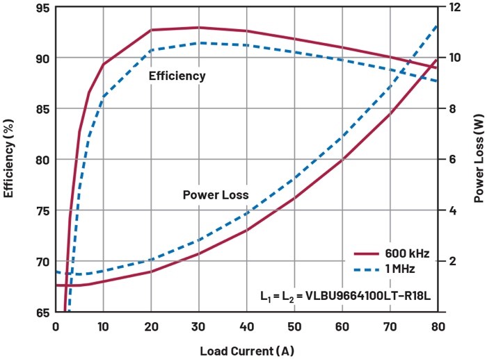
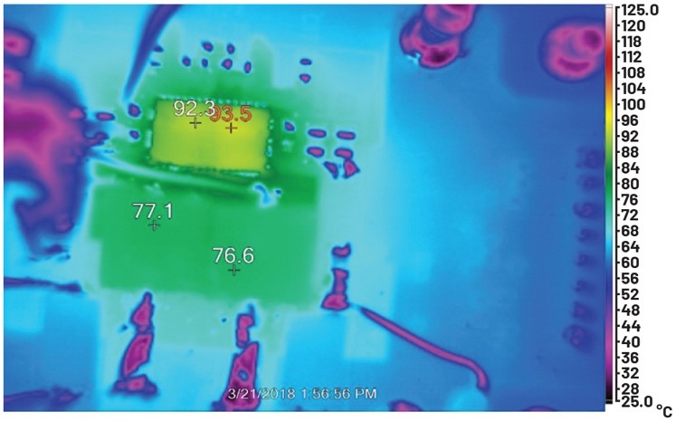
For the 1 MHz design shown in Figure 4, the efficiency at 60 A is almost 90%, while the total power loss, including the inductor loss, is less than 7 W. LTC7050’s thermally enhanced 5 mm × 8 mm LQFN package has a low 10.8°C/W thermal impedance. Its low loss and low thermal impedance enable LTC7050 to replace two industry-standard 5 mm × 6 mm DrMOS modules. Figure 5 shows the thermal image of LTC7050 at 12 V to 1 V/60 A conversion switching at 1 MHz. The case temperature rise over temperature is about 68°C.
Rigorous Fault Alert and Protection System Ensures the Safety of the Load
The LTC7050 family incorporates an array of fault detection, alert, and protection features to ensure the safety of the system.
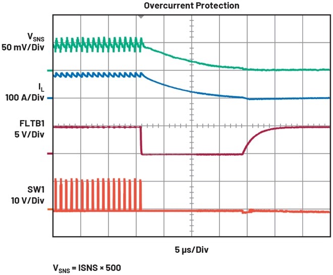
LTC7050 has a fully tested overcurrent protection for both top and bottom FETs. Matching devices on the same die as power devices extract the instantaneous current flowing through the power FETs. The monolithic architecture guarantees that temperature and process variation effects are well canceled, with negligible parasitic effects causing a delay of current sensing signals. These intrinsic advantages of monolithic architecture realize real-time, precise current monitoring and protection. Once the overcurrent comparator is tripped, the affected power device is latched off regardless of the PWM input, the FLTB pin is pulled low to report the fault to the controller, and the opposite device is turned on to freewheel the inductor current to zero. The drivers only accept PWM signals again after the current ramps down to zero. This protection scheme prevents the power stage from continuously chattering around the positive or negative current limit, averting thermal stress on the devices. Figure 6 shows the effect of ramping up load current until the positive overcurrent protection is invoked.
To guarantee that the power devices stay within their safe operating areas, LTC7050’s input overvoltage lockout feature forces both power switches to stop switching when the input voltage is beyond the OV threshold. If the power MOSFET is carrying large current when the OV is detected, then the current is freewheeled by the opposite power device as described above.
The LTC7050 family provides two temperature measurement interfaces to the controller (like LTC3884) or system monitor. The TDIODE pin connects to a PN junction diode to measure the IC junction temperature using VBE method or ΔVBE method. TMON is a dedicated pin to report the die temperature with an industry-standard 8 mV/°C slope. Unlike a standard DrMOS module, which combines analog temperature monitoring with other fault alerts in one pin, LTC7050 TMON is pulled to VCC only if the die temperature is at least 150°C; under other fault conditions, TMON will keep reporting the die temperature while the FLTB open-drain output is pulled low. The monolithic architecture allows TDIODE and TMON to closely reflect the power devices’ temperature. When multiple power stages are employed in a high phase count system, the TMON pins can be connected to report the highest temperature.
Integrating the bootstrap diode and bootstrap capacitor into the package eliminates the need for a boost pin, as well as the chance of accidentally shorting the bootstrap driver. Internally, the bootstrap driver voltage is continuously monitored. If the voltage falls below the undervoltage threshold, then the top FET is turned off to avoid excessive conduction loss.
Conclusion
LTC7050 SilentMOS monolithic high current smart power stages are an ideal solution for high-frequency point of load applications. The symmetrically placed, integrated hot loops bring a number of benefits. Having fewer external components reduces external component count, shrinks the PCB footprint, and lowers bill of material costs. The low switch node ringing enhances the reliability of the device. Low switching related loss offers high efficiency at high switching frequency, permitting the use of small inductors and shrinking the size of the output capacitor since the closed-loop bandwidth is higher. Comprehensive monitoring and protection features protect expensive loads under various fault conditions.
Contributory Authors: