The Paper Explores Ways to Leverage 3D Technology’s Strengths for Lowering Device Energy Consumption and Energy Lost in Data Transmission
CEA-Leti papers confirm the advantages of combining 3D architectures and resistive-random-access-memories (RRAM) for in-memory computing (IMC), and their applications for Edge-AI and neural networks. The projects were designed to look at different ways to leverage 3D’s strengths in lowering device energy consumption as well as energy lost during data transfer.
“Today, storage-class memories like high-density 3D crossbar RRAM are promising for applications requiring a large amount of on-chip memory,” explained the paper 3D RRAMs with Gate-All-Around (GAA) Stacked Nanosheet Transistors for In-Memory-Computing. “RRAM is a leading candidate due to its high density, good scalability, low operating voltage, and easy integration with CMOS devices. Another attractive aspect of RRAM is their ability to perform primitive Boolean logic operations for in-memory and neuromorphic computing. However, if the 1T1R design is the most reliable architecture for IMC, the cell size remains limited by the conventional access transistor.”
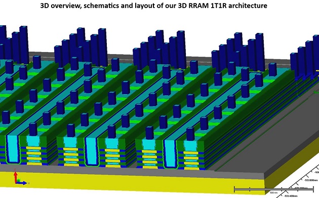
In that paper, scientists proposed a novel 3D memory-cube technology that targets non-volatility, high density, high parallelism of operations and co-integration with CMOS, which makes it very attractive for storage-class memories and IMC. The memory cube is based on a one-transistor / one-RRAM (1T1R) bitcell. 1T1R architecture benefits from the high density of vertically stacked nanosheet (NS) transistors, developed for advanced CMOS, which feature excellent 3D integration scalability.
In the project, CEA-Leti built the technology design foundations (emulation of the process flow, design kit development, bitcell layout and SPICE modelling), which enabled scientists to assess 3D memory topology definition. Then they fabricated key elementary devices: junctionless nano-scaled transistors and HfO2-based OxRAM. Finally, SPICE simulations were carried out to assess the ability of the 3D RRAM cube to perform Boolean operations with up to four operands. This approach co-optimized technology and design together.
One key output of this work is that the estimated bitcell size of (23.9×F2)/N, with “N” being the number of stacked layers, and “F” the minimum feature size. The research results mean that this 1T1R technology is competitive with crossbar memory density when the number of stacked layers is higher than six. The energy of a Boolean operation performed directly in this memory cube is in the nanojoul (nJ) range, with up to four operands. The research team also compared different methods to program the memory and compute the data – and demonstrated that a “double coding” scheme is two times more energy efficient than a write-verify approach.
“The 3D 1T1R memory cube built in the project marked the first time this technology has been proposed combining two emerging technologies, GAA stacked nanosheet transistors and RRAMs,” said Sylvain Barraud, an author of the paper. “This opens the way towards a closed integration of high-end logic and high-density, non-volatile memory on the same chip.”
The second paper, High-Density 3D Monolithically Integrated Multiple 1T1R Multi-Level-Cell for Neural Networks, presented a CEA-Leti project that combined a 3D monolithically integrated transistor with RRAM featuring multi-level cell (MLC) programming. The work demonstrated that 3D monolithically integrated, multiple 1T1R structures combined with MLC programming can achieve up to nine conductance levels per RRAM. It is thus possible to store information with a density 4.75x higher than a standard 1T1R planar RRAM cell.
The main goals of this research were to find the limits of MCL programming, and to achieve high-density RRAM arrays using MLC and 3D technology.
“The team showed that by using extensive characterization at the array level, conductance relaxation after MLC programming is the limiting factor for storage applications, rather than device-to-device or cycle-to-cycle variations,” said Eduardo Esmanhotto, an author of the paper. “This phenomenon limits storage to 2-bit per RRAM for such applications. Conversely, neural network inference is resilient to relaxation and therefore it is advantageous to program nine levels per RRAM, equivalent to 3.17 bits.”
Elisa Vianello, Edge AI program manager at CEA-Leti, said the two papers confirm that combining 3D architectures and RRAM for IMC enables development of low-power hardware for AI applications. Using a transistor as the access device instead of a back-end selector is a more mature and reliable solution for IMC and MLC programming. In addition, 3D integration also provides an answer to the problem of the access transistor limiting the size of the memory cell.
For more information: www.cea.fr/english


