


 is a technique used during chip design to ensure that a device can successfully be manufactured at high yield.)
Jacky (Shih-Hao) Huang, Senior Manager, Semiconductor Process & Integration, Asia, Lam Research
- Virtual process development tools can accelerate the identification of process hotspots
- These techniques lead to cost savings and improved yields in chip manufacturing
Design rule checking (DRC) is a technique used during chip design to ensure that a device can successfully be manufactured at high yield. Design rules are established based on the limits and variability of equipment and process technologies in use. DRC checking ensures that a design meets manufacturing requirements and will not result in a chip failure or DRC “violation.” Common DRC rules include minimum width and spacing requirements, misalignment checks, and other specifications to avoid shorts, opens, excess material problems, or other device failures during manufacturing.


At advanced semiconductor technology nodes, the number and complexity of DRC rules increase, and traditional two-dimensional (2D) DRC cannot identify all hotspots and failures. 3D failures are often identified late in the development cycle when using 2D DRC, due to an inability to model or anticipate 3D rule violations. Using silicon fab data and test macros alone to identify late-stage development failures is both time-consuming and costly.
Lam Research’s SEMulator3D virtual fabrication platform can be used to perform 3D modeling and rules-based metrology of semiconductor devices, and to identify hotspots (DRC violations) and potential failures faster and at a lower cost than silicon wafer-based experimentation.
Large area analysis (LAA) is a powerful concept in semiconductor engineering research and development. LAA are sets of experiments that can be used to explore the sensitivity of a potential hotspot and its effect on downstream process steps across a large chip area. A well-designed LAA can help an engineer develop an optimal semiconductor process using a limited number of experimental wafer runs.
However, in semiconductor design and fabrication, the LAA (or experimental) space is not usually fully explored by engineers due to the complexity of potential process issues across a large chip area.
In this article we demonstrate how SEMulator3D virtual fabrication can be used in large area analysis, and demonstrate our methodology by identifying 3D weak points in a large simulation domain.
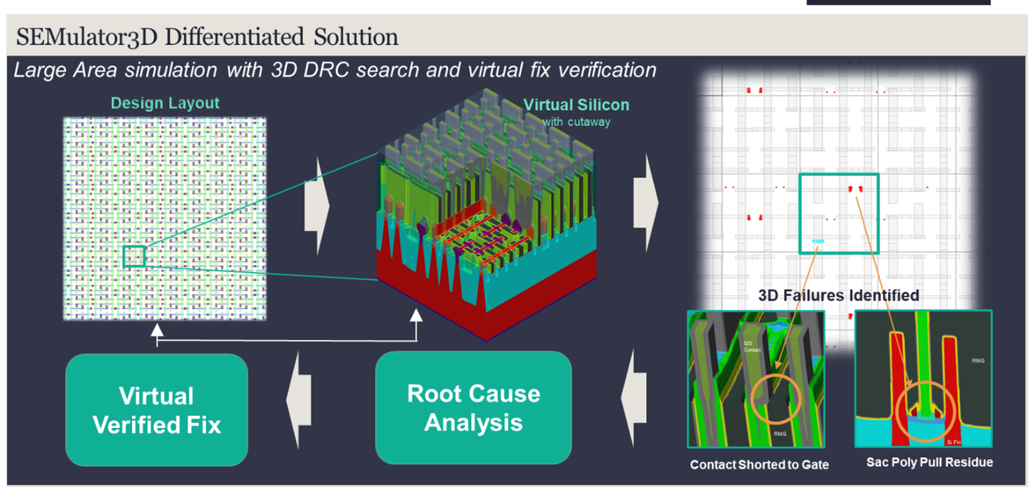
Figure 1: Large Area Analysis (AAA) using SEMulator3D
Large Area 3D DRC Integrated Flow
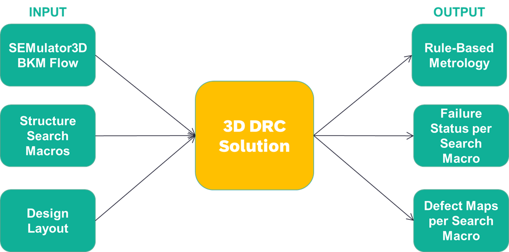
Figure 2 displays a process diagram of a Large Area Analysis (LAA) 3D Design Rule Check (DRC) integrated process. There are three inputs: a SEMulator3D BKM (Best Known Methods) process step model, structure search macros configured with specific defect search criteria, and a design layout.
SEMulator3D is able to use these inputs to identify 3D device failures such as shorts, opens, excess material problems, and others through 3D predictive process modeling. Outputs from this simulation include Rule-Based Metrology, failure identification (from search macros), and the production of defect maps.
After the LAA process is complete, a user can review metrology results for the entire large area simulation domain. In addition, a GDS layout file containing potential weak points is produced for further review.
In the following sections, we will review each of the outputs of the LAA 3D DRC integrated process, and how they can accelerate hotspot and failure identification during semiconductor development.
Rule-Based Metrology With 3D Structure Search
A SEMulator3D 3D model can be used to search for and verify problem areas or hotspots by applying rules-based virtual metrology across the 3D structure. When metrology rules are violated, they can be highlighted in the software. These metrology violations may or may not be recognized during a 2D DRC process. Although certain hotspots can be identified using simple 2D DRC, these results are not complete due to process variability in deposition, etch, or other lithography processes that are not reflected in 2D DRC.
3D process modeling includes both process and structure information and can be used to highlight structural issues, such as minimum insulating distance, contact area overlaps, or other yield-limiting design problems (Figure 3). Geometric criteria can be established during the 3D modeling process to investigate min/max CDs for a variety of device features, along with material interface issues and other device studies. This information can be used to assist in process/design co-optimization efforts and in variability reduction. Virtual and rules-based metrology, combined with 3D structure search, can precede silicon fab data and test macros to identify potentially yield-limiting failures early in the development cycle.
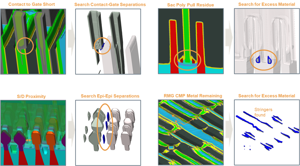
Search Macros and Defect (Hot Spot) Maps
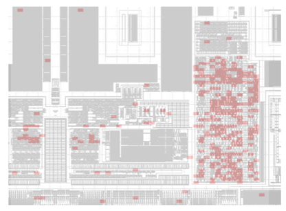
Search macros are able to look across a large semiconductor area in SEMulator3D and identify rules violations or potential future device failures. When search macros identify a failure (using rules-based metrology), the results are automatically output into a GDS file (Figure 4) that displays identified failure locations. The GDS file contains failures and defects identified during the structure search process. These defects cannot normally be found using 2D DRC methodologies, because the defects are 3D in nature. Depending on the type of defects present in the large area study, process model calibration in SEMulator3D may be required to verify predictive accuracy. In principle, advanced calibration is not required to identify unexpected defects.
Conclusion
Identifying process hotspots without requiring wafer-based experimentation is extremely valuable. It leads to savings in wafer and mask costs, and more importantly it accelerates the yield ramp curve for any given technology development.
In a recent program using SEMulator3D, the Large Area Analysis solution identified multiple mask defects early in the development cycle; two of which were corrected, and new masks were ordered. This identification of mask failures could have taken months and many coupon tests to identify without the use of virtual process development tools.
As semiconductor technology advances, LAA techniques are being used to improve yield by minimizing systematic, random, and parametric defects, primarily through the prevention, detection, and repair of projected hotspots. LAA for manufacturability will be a key success factor for companies that wish to succeed in achieving on-time delivery of new semiconductor products.