

 semiconductors are semiconducting materials with thicknesses on the atomic scale, which have exceptional)
Two-dimensional (2D) semiconductors are semiconducting materials with thicknesses on the atomic scale, which have exceptional electronic properties. In the future, these materials could have the potential to replace silicon in the development of numerous electronic and optoelectronic devices.
Despite their advantages, the use of 2D semiconductors has so far been limited, partially due to their low carrier mobility at room temperature. This is caused by a strong scattering of phonons (i.e., quasiparticles associated with collective atomic vibrations) in the materials’ lattices.


Researchers at the Agency for Science, Technology, and Research (A*STAR) in Singapore and The Hong Kong Polytechnic University in Hong Kong, China has recently devised a design strategy that could help to overcome this limitation, improving the carrier mobility of 2D materials. Their proposed approach entails the introduction of lattice distortions in a 2D material, using bulged substrates.
“Our research was inspired by the high carrier mobility observed in 2D TMDs on substrates with high surface roughness by Tao Liu et al. back in 2019,” Dr. Ming Yang and Dr. Jing Wu. Two of the researchers who carried out the study. “However, the observed mobility enhancement was simply attributed to strain effects and the fundamental mechanism remains unclear. To this end, we dug deeper to unravel the underlying physics responsible for such a significant enhancement in mobility and demonstrate lattice engineering as an effective strategy to create high-performance electronic devices at room temperature.”
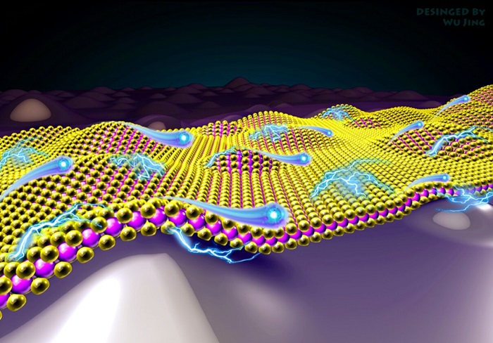
Most conventional strategies for improving the carrier mobility of 2D semiconductors rely on attaining ideal lattice structures. The strategy proposed by Yang, Wu, and their colleagues, on the other hand, merely entails the introduction of bulged substrates, which create ripples in a 2D semiconductor and suppress the scattering of phonons.
“We simply placed 2D materials on substrates with bulged morphologies, creating ripples in the material that leads to lattice distortion,” Yang and Wu explained. “Typically, lattice distortions are slated to adversely affect carrier mobility. However, we show that such lattice distortions create a larger electric polarization, which can not only renormalize the frequency of phonons to effectively suppress scattering between electrons and phonons, but also enhance the intrinsic dielectric constant to further screen the polar phonon scattering.”
Compared to other existing approaches for increasing carrier mobility in 2D semiconductors, the strategy proposed by these researchers is both simple and cost-effective. As part of their study, the team tested it on 2D molybdenum disulfide (MoS2) and found that it resulted in room temperature carrier mobility of approximately 900 cm2 V−1 s−1, which exceeds the predicted phonon-limited mobility of flat MoS2 (ranging between 200 and 410 cm2 V−1 s−1).
“The observed mobility enhancement and the underlying mechanism of such high carrier mobility in rippled-MoS2, which exceeds the predicted phonon-limited mobility in flat-MoS2, is particularly noteworthy,” Yang and Wu said. “Such high carrier mobility can pave the way for low-powered electronics and is an important parameter for most applications ranging from field-effect transistors to photodetectors and more.”
The study carried out by this team of researchers highlights the huge potential of lattice engineering strategies for enhancing the performance of electronics and thermoelectric devices at room temperature. In the future, their method could be used to create more efficient devices based on 2D semiconductors. In addition, it could potentially inspire the development of other design strategies based on lattice engineering.
“In our next studies, we plan to systematically create rippled/bulged substrates to minimize variability, as well as to study the correlations between bulges,” Yang and Wu added.