


Industry 4.0 combines digital world and physical world in which Image sensors have established themselves as a sensory organ. As world is heading towards automated manufacturing, some top notch companies are also ready to bridge the gap between the two worlds. Let us read the Technological advancement, R&D and products the image sensors companies have to offer their customers.

Left to Right: Vishal Malhotra, National Sales Head, Automotive Infineon Technologies, India | Sanjay Jain, Analog Applications Manager, Texas Instruments India | Michael DeLuca, Go To Market Manager, Image Sensor Group, ON Semiconductor | Channabasavaraj Raravi, Senior Solution Architect – Software, Sasken Technologies Ltd
Technology Offered For Image Sensors
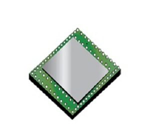
Infineon : Infineon’s Time-of-Flight (ToF) based Image Sensor family REAL3 paves the way for numerous applications and innovations not previously possible. The technology is helping us to meet the growing demand in numerous applications in consumer, industrial and automotive segments.

REAL3 Image Sensor family brings together all necessary ingredients to establish 3D image. Brightness and the distance from the sensor to objects are measured in every single pixel. The 3D camera emits modulated infrared light and measures the time the infrared signal takes to travel from the camera to the object and back again: “time of flight” refers to the elapsed time. This helps to provide robust and accurate depth data.
 Texas Instruments: Texas Instruments has come out with next generation technology of 3D Time of Flight sensing Analog Front End Devices which completely change the gambit of Image Sensing Applications. This technology relies on capturing and processing 3D map (X,Y,Z) of the object; commonly referred to as “Point Cloud”. It employs IR (Infrared) as a medium to measure distance by emitting a modulated light and measuring phase delay of returned light, in IR spectrum. This enables to capture the 3D map of the object. This is called as 3D Point Cloud Information. An array of pixels are used to map a region of interest for getting this 3D Point cloud.
On-Semiconductor: ON Semiconductor provides a full portfolio of image sensors based on both CCD and CMOS technologies that are used in applications ranging from machine vision inspection and automotive ADAS to surveillance, consumer, and medical imaging. Our 40 year legacy of image sensor development allows us to leverage technologies such as advanced pixel designs, high bandwidth outputs, electron multiplication, packaging options, customized color filter array patterns, and more to provide unique solutions to our customer’s most demanding imaging problems.
Sasken: The current focus from Sasken is in the Automotive and Retail domains. The automotive domain requires real-time processing of images. We are currently focused on making some tiny real-time algorithms to do application specific image processing for Autonomous cars. The current challenge in Autonomous driving is the testing of different image processing algorithms. This also needs special skillset to do verification of different algorithms with various combinations of images. The test automation is another focus area where a larger number of test cases could be tested within short span of time and with good quality. The Retail segment (specifically Fashion) requires the image super imposition capability to realise virtual shopping or virtual trial rooms.
Uniqueness of Image Sensor
Infineon: ToF method of depth measurement incorporated into the highly optimized REAL3 Image Sensors offers many benefits compared to other depth sensing technologies, ToF offers advantages in performance, size and power consumption of battery-operated mobile devices. ToF based Image Sensor family REAL3 is sunlight robust, highly scalable, and ready for integration. According to the Global Image 3D Sensors Market 2017, Infineon Technologies is the top seller of the 3D Sensor technology.
Texas Instruments: Image Sensor AFEs helps to capture complete 3D Point cloud, it enables solving a wide array of existing challenges in Machine vision with relatively minimal effort in terms of implementation. Rather than implementing a 2D Stereoscopic Image stitch to extract 3D point cloud information, this technology works on IR transmission from a Modulated Light Source and reception through a IR Photo Diode and then extracting object information in a 3D point cloud format. More importantly, if you benchmark this technology on parameters of low light condition imaging, Distance Range, depth accuracy, it performs well as compared to a existing solution set. Also, given the implementation, this solution is lot reliable and can prove boon for SIL certification for Factory Automation Applications. Applications involving privacy concerns would immensely benefited from this technology as it only captures 3D point cloud information and not actual image.
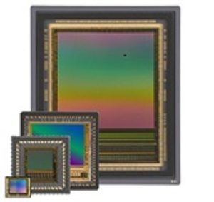 On-Semiconductor: Clearly, the first differentiator is the unique set of base technologies available to develop the image sensors in our portfolio, such as the advanced global shutter pixel architectures and Interline Transfer EMCCD designs mentioned above. These technology components are then leveraged into a broad portfolio of over 1000 different orderable devices, with pixel sizes ranging from 1 to 25 microns, resolutions from VGA to 50 megapixels, and with options for different packaging configurations, optical format, light sensitivity, power requirements and more – providing an unparalleled opportunity to select the most appropriate image sensor for a particular application.
But we then go beyond these separate elements to design product families that leverage these base technology packages into an integrated portfolio – allowing camera manufacturers to leverage a single camera design to provide a full portfolio of cameras with different resolutions, light sensitivities, and package configurations. This family architecture design simplifies the work need by camera manufacturers to develop and support new camera designs, allowing them to bring cameras to market more quickly and cost effectively.