.")
In the context of electrical and electronic engineering, a switch is a component that can “make” or “break” an electrical circuit, thereby interrupting an electric current or diverting it from one conductor to another. As engineers can attest, there are many different types of switches including toggle switches, rocker switches, pushbutton switches, micro and limit switches, magnetic and reed switches, and relays. All have one thing in common: they bounce. It’s just what they do.
Ordinarily, this bounce has little or no effect on the circuit, but if the digital circuit is fast enough to detect and respond to multiple bounces, there can be serious consequences. An engineer’s task is to avoid or mitigate the effects of this bounce, or “debounce” the switch. While the industry has long practiced hardware debounce, it has more recently moved to software-based debounce approaches. However, there are situations where hardware debounce is a better option.


This article explains bounce and discusses software and hardware approaches to debounce. It then points to instances where hardware debounce is a better option before showing how it can be implemented. Example switching devices and hardware debounce components are introduced by way of examples from NKK Switches, ON Semiconductor, Texas Instruments, Maxim Integrated, and LogiSwitch.
What is switch bounce?
When a switch or relay is flipped or toggled, what a human perceives as being an instantaneous single response each time the device changes state may actually involve 100 or more make-or-break actions that persist for several thousandths of a second before the contact finally settles in place.
For example, consider a single pole, single throw (SPST) normally open (NO) panel mount toggle switch like an M2011SS1W01 from NKK. Assume that one side of this switch, which can be considered the input, is connected to ground (0 volts), while the other side, which in this case is the output, is connected to a 5 volt power supply (shown as +ve) via a pull-up resistor (R1) (Figure 1).
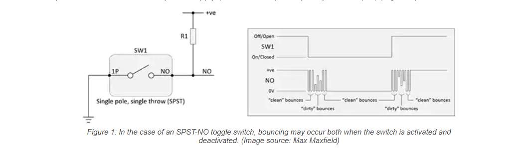 Observe that switch bounce may occur both when the switch is activated (closed) and deactivated (opened). Sometimes the bounces may transition all the way between the supply rails, here considered logic 0 and 1 states. In this case, these are “clean” bounces. By comparison, if the signal reaches only an intermediate voltage, these are referred to as “dirty” bounces.
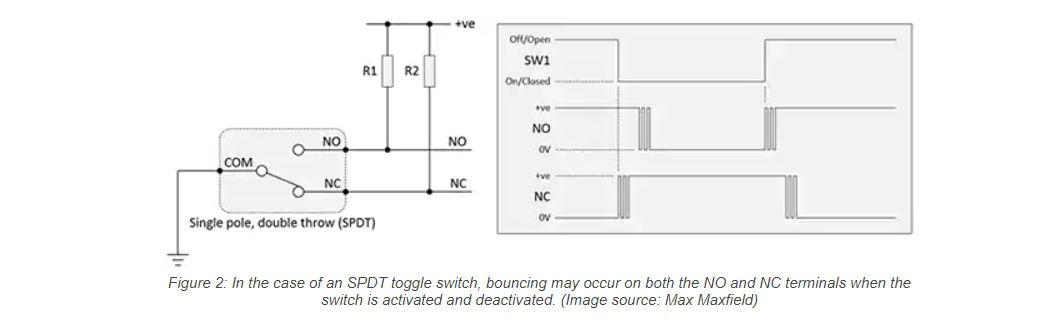
In the case of a single pole, double throw (SPDT) panel mount toggle switch like NKK’s M2012SS1W01-BC, bouncing may occur on both the normally open (NO) and normally closed (NC) terminals (Figure 2). In this case, only “clean” bounces have been shown for simplicity.
 In many cases, this signal bounce duration is such that it has no effect. Problems arise when a switch is connected to a piece of electronic equipment that is fast enough to detect and respond to multiple bounces. What is required is a way to debounce the signal coming from the switch before it is acted on by the electronic equipment.
Software versus hardware debounce
In the 1960s and 1970s, switch debounce was implemented using a variety of hardware techniques, from simple resistor-capacitor (RC) delay circuits used with SPST switches to more sophisticated set/reset (SR) latch functions.
More recently, and because many systems feature a microprocessor unit (MPU) or microcontroller unit (MCU), it has become commonplace to use software techniques to debounce the signal coming from any switch. However, software debounce is not always the best approach. There are some applications that involve small, low-performance, memory-constrained processors with limited code space and/or clock cycles available to implement debounce routines. In these instances, a hardware implementation may be a better solution.
Also, many software developers are unfamiliar with the physical characteristics of switches, such as the fact that in addition to varying from one activation to another, the bounce characteristics of a switch may be affected by environmental conditions like temperature and humidity.
The issue of software developers’ lack of switch expertise is exacerbated by the fact that available literature regarding switch bounce is often confusing and contradictory. For example, it’s common to read that a switch will have stopped bouncing 1 millisecond (ms) after its activation or deactivation. However, well-known embedded systems expert Jack Ganssle performed empirical tests on a variety of switch types, activating each switch 300 times and logging the minimum and maximum amount of bouncing for both the opening and closing of the contacts.
He reported an average bounce duration of 1.6 ms and a maximum bounce duration of 6.2 ms. Some industrial and military “best practices” recommend waiting 20 ms after initial activation before assuming the switch has stopped bouncing; others advocate waiting 20 ms following the final detected bounce before triggering any actions.
Furthermore, there are many simple non-processor-based systems that also require switches to be debounced. A few examples of such systems are a binary counter driving seven-segment displays counting pulses from a relay; the trigger input to a 555 one-shot timer being used as a motor control for a door or gate; and a register-based finite state machine (FSM) that employs keyed inputs. There are also electronic trim potentiometers (pots) with values modified using switch inputs (up, down, and sometimes store) where switch bounce would be problematic.
All of these examples make it clear that some knowledge of how to perform hardware debounce can be useful for any designer or developer.
Hardware debouncing an SPST switch with an RC network
One of the simplest hardware-based switch debounce solutions employs a resistor-capacitor (RC) network in conjunction with an SPST switch. There are many variations of such a circuit. One of the more versatile implementations involves two resistors and a diode (Figure 3).
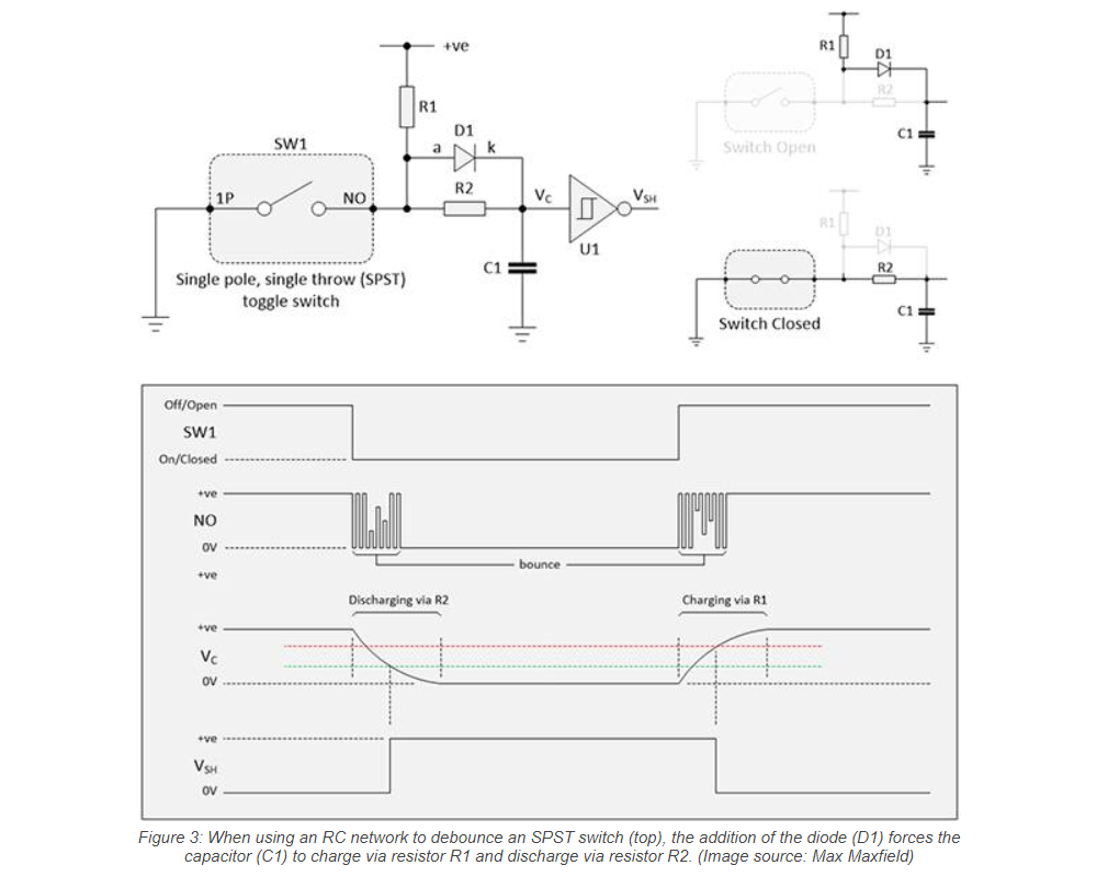 When the switch is activated (closed), capacitor C1 is discharged via resistor R2. If diode D1 had been omitted from this circuit, then when the switch was deactivated (opened), C1 would be charged via resistors (R1 + R2). However, the presence of D1 means that C1 will be charged only via R1.
In some cases, only the activation of the switch is of interest (i.e., triggers actions to occur), in which case D1 may be omitted. However, if actions are to be triggered when the switch is both activated and deactivated, and if minimizing delay is a consideration, the addition of D1 is recommended.
Observe the exponential charging and discharging curves exhibited by the capacitor voltage VC. It would not be a good idea to feed this signal directly to the input of a downstream digital logic function, which wouldn’t appreciate seeing a signal that dawdles in the undefined region between “good” logic 0 and logic 1 values. Instead, this signal is fed to the input of a buffer with a Schmitt trigger input. Furthermore, an inverting buffer is typically used, such as one channel of a CD74HC14M96 from Texas Instruments, because inverting functions switch faster than their non-inverting counterparts.
Debouncing an SPDT switch with an SR latch
In the case of an SPDT switch, a common hardware debounce solution is to employ an SR latch. Ever since companies like IBM used this technique for the switch panels on their mainframe computers circa the 1960s, this approach has been regarded as the crème de la crème of simple hardware debounce solutions. Such a latch can be formed using two back-to-back two-input NAND gates; for example, by employing two channels of an SN74HC00DR quad two-input NAND IC from Texas Instruments (Figure 4).
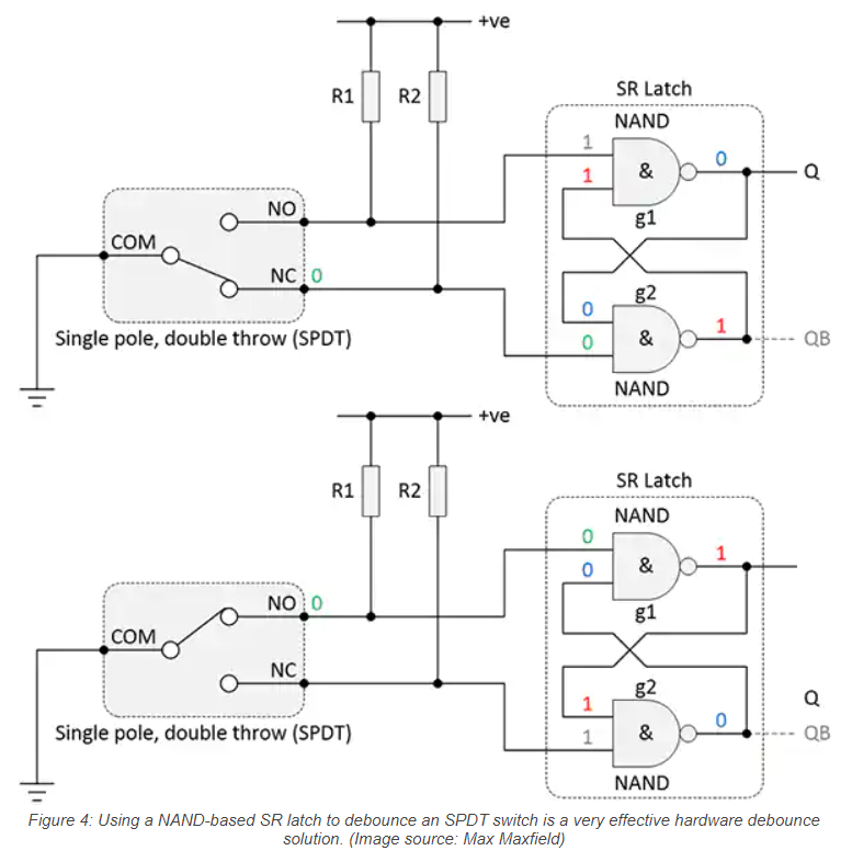 When the switch’s NC terminal is connected to ground, as shown in the upper half of Figure 4, this forces the output of gate g2 to logic 1. In turn, the two logic 1s on the inputs to gate g1 force its output to logic 0. By comparison, when the switch’s NO terminal is connected to ground, as shown in the lower half of Figure 4, this forces the output of gate g1 to logic 1. In turn, the two logic 1s on the inputs to gate g2 force its output to logic 0.
The reason this circuit works so well is that when both of its inputs are in their inactive logic 1 states, the SR latch remembers its previous value. Remember that as illustrated in Figure 2, when an SPDT switch is toggled, whichever of its terminals is connected to ground at that moment in time bounces first. Since these bounces are between its original value (logic 0) and its new value (logic 1), they have no effect on the current state of the SR latch. It’s only after this terminal ceases to bounce that its counterpart starts to bounce, at which time the SR latch changes its state.
Debouncing an SPST switch with a dedicated device
One problem with the previous solution is that many designers prefer to use SPST switches because they generally cost less than SPDTs. There are a number of well-known dedicated SPST debounce devices on the market, such as the MC14490DWG from ON Semiconductor and the MAX6818EAP+T from Maxim Integrated.
Another manufacturer, LogiSwitch, offers a suite of three-channel, six-channel, and nine-channel debounce solutions in both through-hole and surface mount device (SMD) packages. For example, consider a circuit using a LogiSwitch LS18-S device (Figure 5).
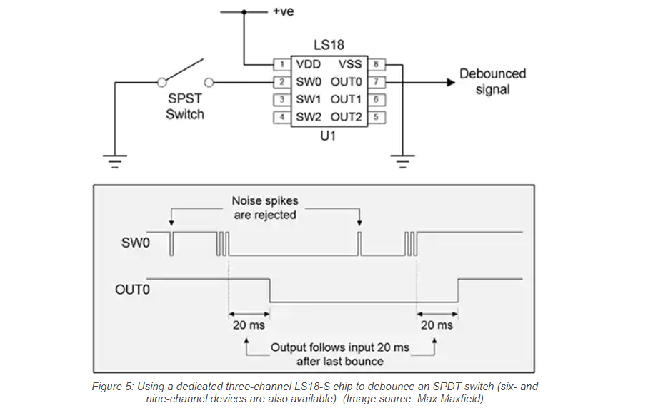 Like all members of the LogiSwitch family, the LS18-S supports an operating voltage range of 2.5 to 5.5 volts (the value of the supply voltage does not affect the device’s response time). Also, unlike some of the other dedicated IC solutions, LogiSwitch debounce devices do not require any additional components such as an external clock, an RC timing network, or pull-up resistors on the inputs or outputs.
The LS18-S uses LogiSwitch’s proprietary adaptive NoBounce technology, which offers a high level of noise immunity. Noise spikes of less than 20 ms duration are prohibited from starting or terminating a cycle, and outputs are delayed for a period of 20 ms following the final switch bounce on both activation and release regardless of the bounce duration.
Conclusion
There are many different types of switches, including toggle switches, rocker switches, and pushbutton switches, all of which may bounce. If unmitigated, switch bounce can cause microprocessors and other electronic circuits to see a single switch activation as comprising multiple events.
The bouncing signal from a switch is often debounced using software running in a microcontroller. Although this is a low-cost solution, as shown, it may not be the best option in all cases, including systems based on performance and memory-limited microcontrollers, software developers lacking expertise in switch-related issues, or systems implemented without a microcontroller.
As an alternative, debouncing may be performed in hardware using a variety of approaches ranging from resistor-capacitor networks to SR latches to dedicated integrated circuits.