

Engineering researchers have created new high-power electronic devices that are more energy efficient than previous technologies. The devices are made possible by a unique technique for “doping” gallium nitride (GaN) in a controlled way.
“Many technologies require power conversion—where power is switched from one format to another,” says Dolar Khachariya, a researcher on the work and a former Ph.D. student at North Carolina State University. “For example, the technology might need to convert AC to DC, or convert electricity into work—like an electric motor. And in any power conversion system, most power loss takes place at the power switch—which is an active component of the electrical circuit that makes the power conversion system.”


“Developing more efficient power electronics like power switches reduces the amount of power lost during the conversion process,” says Khachariya, who is now a researcher at Adroit Materials Inc. “This is particularly important for developing technologies to support a more sustainable power infrastructure, such as smart grids.”
“Our work here not only means that we can reduce energy loss in power electronics, but we can also make the systems for power conversion more compact compared to conventional silicon and silicon carbide electronics,” says Ramón Collazo, researcher and an associate professor of materials science and engineering at NC State. “This makes it possible to incorporate these systems into technologies where they don’t currently fit due to weight or size restrictions, such as in automobiles, ships, airplanes, or technologies distributed throughout a smart grid.”
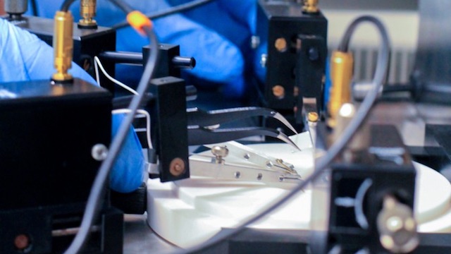
The researchers outlined a technique that uses ion implantation and activation to dope targeted areas in GaN materials. In other words, they engineered impurities into specific regions on GaN materials to selectively modify the electrical properties of the GaN only in those regions.
In their new paper, the researchers have demonstrated how this technique can be used to create actual devices. Specifically, the researchers used selectively doped GaN materials to create Junction Barrier Schottky (JBS) diodes.
“Power rectifiers, such as JBS diodes, are used as switches in every power system,” Collazo says. “But historically they have been made of the semiconductors silicon or silicon carbide because the electrical properties of undoped GaN are not compatible with the architecture of JBS diodes. It just doesn’t work.”
“We’ve demonstrated that you can selectively dope GaN to create functional JBS diodes and that these diodes are not only functional but enable more power efficient conversion than JBS diodes that use conventional semiconductors. For example, in technical terms, our GaN JBS diode, fabricated on a native GaN substrate, has record high breakdown voltage (915 V) and record low on-resistance.”
“We’re currently working with industry partners to scale up production of selectively doped GaN, and are looking for additional partnerships to work on issues related to more widespread manufacturing and adoption of power devices that make use of this material,” Collazo says.