


Description
This automotive reference design is based on TI’s Jacinto DRA71x processor and focuses on system level cost savings. The six-layer design reduces PCB costs through optimized via breakout scheme and power distribution network as well as integration of key features. Functionality can be added or removed based on the end product requirements. This design targets applications such as infotainment and reconfigurable digital cluster. The design has a 12- V input with a single PMIC. The design supports HDMI, USB3.0 or USB2.0, TAS6424 digital Class-D amplifier, FPD-Link interface, and many other features. A Linux, Android, or QNX based software development kit (SDK) is included.


 Features
- TI Jacinto DRA71x Processor With Integrated Features Help Design Cost-Effective, Feature Rich, Entry Level (Display Audio) Infotainment and Cluster Systems
- DRA71x Superset Processor With 2D and 3 D graphics, C66x DSP, and Cortex-M4 options
- Processor SDK for Linux, Android, and QNX Development With Add-on Packages for Radio and Audio
- Cost Saving Features Include Six-Layer HW Design, Rear-View Camera (RVC) Support, Tuner Integration with Software Defined Radio (SDR), Class-D Amplifier and Multi-Sone Audio Support
- Includes TI’s Solution and Support for Power, Audio, Processing, and Display
Applications
- Entry Level In-Vehicle Infotainment (IVI) Head Unit
- Digital Cluster
- Radio and Audio Co-processor
- Automotive Amplifier
 1 System Description
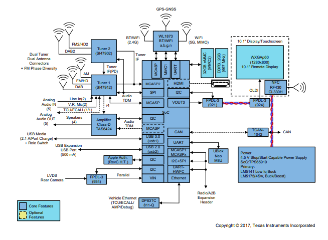
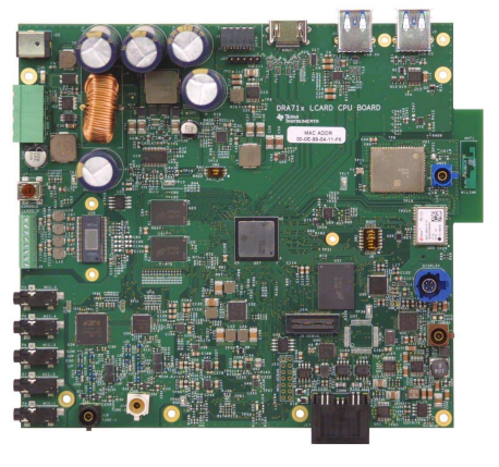
This reference design is a system that includes the DRA 71x automotive applications processor, a power solution, DRAM(DDR3L), and multiple interface ports an expansion connectors. This system is designed on a six-layer PCB using a unique via breakout scheme, a single PMIC solution, and fewer but integrated functions that allows for lower manufacturing costs without sacrificing quality of the end product. The reference design targets entry level infotainment applications with a high-end look and feel. An HDMI and FPD-Link III port allows for the connection of a high-definition display and rear view camera to provide a rich user interface. A Bluetooth and Wi-Fi module, audio and tuner inputs, and USB port are included to allow for connectivity of wireless and wired audio devices for rich output from the Class-D audio amplifier. The optimized power solution allows the design to be powered from a single 12-V power source.
1.1 Key System Specifications
Table 1. Key System Specifications
| PARAMETER | SPECIFICATIONS | DETAILS |
| Input power source | 12-V power adapter or variable power source | Section 3.1.1 |
| Start-stop | System can run as low as 6V when engine starts | Section 2.2.4 |
| Battery dropout support | System has 50ms of backup support in case of loss of power | Section 2.2.3 |
| Class-D audio amplifier | Audio output from input stream | Section 2.2.6 |
| Global positioning system (GPS) | Module option for GPS, Bluetooth, or Wi-Fi | Section 2.2.7 |
| TPS65919 PMIC | Single-power solution for SoC | Section 2.3.2 |
| Six-layer PCB design | Lower-cost PCB solution | Section 2.4.1 |
2 System Overview 2.1 Block Diagram
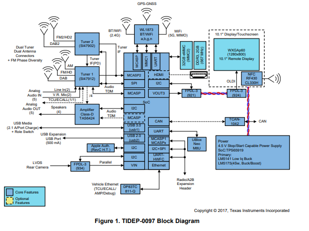
2.2.1 DRA71x Applications Processor
This reference design uses the DRA71x application processor to integrate and handle all the peripheral inputs and to deliver the outputs to the respected ports. Included features are RVC and SDR capabilities, which take away the requirement for discrete components because they are included in the SoC of the DRA71x. The device features a simplified power supply rail mapping, which enables lower cost PMIC solutions.
2.2.2 Power Architecture
This reference design has optimized power architecture. The input to the design can be a 12-V power source similar to a car battery. The 12-V source is boosted to 16 V and is also bucked down to 3.3 V. The 16 V is used for the media hub, display module, and local USB port. The 16 V is also bucked down to 10.5 V to be used for sensor ports and modules. The 3.3 V is the input to the TPS65919-Q1, which provides a single PMIC power solution for the design. The TPS65919 PMIC is optimized to provide all the power rails for the SoC.
2.2.3 Battery Dropout Protection
This design includes battery dropout protection in case the battery suddenly becomes disconnected or shorted and causes the voltage to drop to 0 V immediately. This protection provides immunity to momentary voltage dropouts that may occur over the life of the vehicle. If the battery becomes disconnected, this protection is specified to power the downstream power rail for as long as 50 ms in cycles. The four parallel 2200-µF capacitors act as a small battery to provide power during the disconnection time. This feature is optional based on the end product, but removing this feature could result in lower design costs. Refer to Section 23.0 in the FordEMC document.
2.2.4 Start-Stop System
Auto start-stop systems are starting to be widely implemented in infotainment systems.. A start-stop system or stop-start system automatically shuts down and restarts the engine to reduce the amount of time the engine spends idling, which reduces fuel consumption and emissions. This system applies to cases such as stopping at a red light, stop sign, and so forth. When the engine shuts down and resets many times, the battery voltage drops and normally causes the system to lose power frequently.
The reference design has a buck-boost solution using LM5175-Q1 to prevent the system from losing power in these cases. The main specification for the start-stop feature is the system must be able to maintain full functionality all the way down to 6 V while being supplied from the car battery. 6 V is the specification for this design; however, some systems can be designed to be powered with a lower or higher voltage depending on specifications. Some companies require this feature; however, the feature is optional, and if the feature is removed from the design, the removal can reduce cost. Refer to Section 20.0 in the FordEMC document for the timing diagram.
The start-stop feature is end equipment specific. The design can be scaled to leave out the start-stop feature if desired. However, this reference design includes the start-stop feature.
2.2.5 Radio Tuners
The reference design includes an AM, FM, and HD radio receiver to be used in conjunction with the integrated software defined radio. There are two radio tuners in the design: one is only a tuner, and the other is a tuner with an integrated audio CODEC. The single tuner receives the radio signal and sends the signal to the DSP in the SoC for additional processing. The tuner with the built-in CODEC can receive the radio signal and process the signal onsite, which makes this tuner versatile with analog or digital signals and distributes them throughout the audio system. The tuner accepts a coaxial connection that connects to a Rosenberger FAKRA RF connector.
2.2.6 Class-D Audio Amplifier
The TAS6424-Q1 is a digital Class-D audio amplifier designed to provide four channels with 4-Ω output capability with up to 75-W output power. The outputs are placed on the design to connect speakers to resemble a stereo load. Different amplifier solutions are available.
2.2.7 Bluetooth, WLAN, GPS
Wireless connectivity is desired for hands-free infotainment use. This reference design includes wireless connectivity capabilities for Bluetooth, WLAN, and GPS. This design supports Standard Bluetooth, BLE, 2G WLAN, and 5G WLAN on the module. The module is built off the chipset from TI WL1873, which offers integrated Wi-Fi, Bluetooth, Bluetooth Smart, and GPS solutions. The module offers an audio solution for AirPlay receivers, full audio stack streaming, and more infotainment audio streaming options. The WL1873 offers high throughput and extended range with Wi-Fi and Bluetooth coexistence in a power-optimized solution. Only a single dual-band antenna is required for the module. A dual-band 2.4-GHz or 5GHz PCB antenna is used. The WL1873 provides entry-level GPS capabilities. The GPS feature on the WL1873 module supports two of the four GPS satellite constellations, thus making the module a cost-effective solution for entry-level navigation.
There is an option to use a u-blox M8U module that provides a more-accurate GPS feature because the module supports all four of the satellite constellations around the world and offers 802.11ac for Wi-Fi capabilities. The u-blox module is an option that can be added based off of product requirements.
2.2.8 FPD-Link III
The design includes a 720-p FPD-Link III parallel-to-serial interface (DS90UB921). The interface supports up to 24 bits of data and can operate at pixel rates up to 85 MHz. An interrupt is supported to enable the back-channel communication, which is typically required if supporting touch screen capabilities. Power control to the panel is also supported through SoC GPIO. The SerDes pair is designed for a robust, rear view camera peripheral to be included in the system.
2.2.9 High-Definition Multimedia Interface ( HDMI )
The design includes an integrated HDMI interface, which is supported on a type-A HDMI connector. The interface will support 1080 p with 24-b color. A communication channel (DDC/CEC) is supported to the HDMI connector for communication with the HDMI panel. A monitor detect indication is also provided. The DDC/CED interface and monitor detect signals are translated through the transceiver and can be controlled using GPIO from the SoC.
2.2.10 Universal Serial Bus ( USB )
The design includes two integrated USB transceivers. USB3.0 super-speed bus (USB-SS) is supported using port USB-SS to a USB3.0 type-A connector. This interface supports up to 5 Gbps and can operate in host or device mode. Also included is a USB2.0 high-speed interface HUB (USB-HS) and can support rates up to 480 Mbps. All USB interfaces can supply VBUS to peripheral when in host mode by enabling VBUS switch; however, the design cannot be powered from VBUS when in device mode.
2.3 Highlighted Products
This reference design features the following TI devices. Refer to the corresponding datasheets for additional information.
- DRA71x application processor
- TPS65919-Q1
- DS90UB921-Q1
- TAS6424-Q1 or TAS6424L-Q1
- DP83TC811-Q1
- DS90UB934-Q1
2.3.1 DRA71x Infotainment Applications Processor
The DRA71x architecture is designed to deliver high-performance concurrencies for automotive applications in a cost-effective solution, which provides full scalability from the Jacinto6 family of infotainment processors including graphics, voice, HDMI, multimedia, and smartphone projection mode capabilities.
Programmability is provided by a single-core Arm Cortex-A15 RISC CPU with Neon extensions and a TI C66x VLIW floating-point DSP core. The Arm processor allows developers to keep control functions separate from other algorithms programmed on the DSP and coprocessors, which reduces the complexity of the system software.
- Video, image, and graphics processing support:
- Full-HD video (1920 p × 1080 p, 60 fps)
-
- Arm Cortex A-15 microprocessor subsystem
- C66x floating-point VLIW DSP
- DDR3/DDR3L memory interface (EMIF) module
- HDMI encoder
- SuperSpeed USB3.0 dual-role deviceMultiple video input and video output
- 2D and 3D graphics
2.3.2 TPS65919-Q1 Power Management Unit
TPS65919-Q1 PMIC integrates four configurable step-down converters with up to 3.5A of output current to power the processor core, memory, I/O, and pre-regulation of LDOs. The device is AEC-Q100 qualified. The power-sequence controller uses one-time programmable (OTP) memory to control the power sequences as well as default configurations such as output voltage and GPIO configurations. The OTP is factory programmed to allow start-up without any required software.
- Qualified for automotive applications
- AEC-Q100 qualified
- System voltage range from 3.135 V to 5.25 V
- Four step-down switched-mode power supply (SMPS) regulators
- Four low-dropout (LDO) linear regulators
- Power sequence control
2.3.3 DS90UB921-Q1 FPD-Link III Serializer
The DS90UB921-Q1 serializer, in conjunction with DS90UB934-Q1 deserializer, provides a complete digital interface for concurrent transmission of high-speed video, audio, and control data for automotive display and image sensing applications.
- Qualified for automotive applications
- AEC-Q100 qualified
- Supports extended high definition (1920 p × 720 p, 60 Hz) digital video format
- AC-coupled coax or shielded-twisted pair (STP) interconnect up to 10 m
- Single 3.3-V operation with 1.8-V or 3.3-V compatible LVCMOS I/O interface
- TAS6424-Q1 Class-D Audio Amplifier
The TAS6424-Q1 device is a four-channel digital-input Class-D audio amplifier designed for use in automotive head units and external amplifier modules. The device provides four channels at 27 W into 4 Ω at 10% THD+N and 45 W into 2 Ω at 10% THD+N from a 14.4-V supply and 75 W into 4 Ω at 10 % THD+N from a 25-V supply. The Class-D topology dramatically improves efficiency over traditional linear amplifier solutions. The output switching frequency can be set either above the AM band, which eliminates the AM-band interference and reduces output filtering and cost, or below AM band to optimize efficiency.
There is also a pin-for-pin compatible lower-cost solution for the Class-D amplifier. The TAS6424L-Q1 is an identical package amplifier; however, the maximum voltage power is 18 V, the output power to bridge tied load is 27 W, and the power to parallel bridge tied load is 70 W. Compared to the TAS6424-Q1 Class D, the output power is half, which correlates to the lower input voltage.
- DP83TC811-Q1 Automotive Ethernet PHY
The DP83TC811-Q1 is a single-port automotive Ethernet PHY compliant to IEEE802.3bw. The device provides all physical layer functions required to transmit and receive data over single twisted-pair cables. Additionally, the DP83TC811-Q1 provides flexibility to connect to a MAC through a standard MII, RMII, RGMII, SGMII.
- Qualified for automotive applications
- Low active power: 3.3 V VDDA/VDDIO
- Configurable I/O voltages: 3.3 V, 2.5 V, and 1.8 V
- Power saving features
2.3.6 DS90UB934-Q1 FPD-Link III Deserializer
DS90UB934-Q1 deserializer, in conjunction with the DS90UB913A/933 serializers, supports the video transport needs with a ultra-high speed forward channel and an embedded bidirectional control channel. The DS90UB934 converts the FPD-Link III stream into either a parallel CMOS output or MIPI CSI-2 interface designed to support automotive image sensors up to 12 bits at 100 MHz with resolutions including 1080 × 720 at 60 fps. The DS90UB934 chipset is fully AEC-Q100 qualified and designed to receive data across either 50-Ω single-ended coaxial or 100-ΩSTP cable assemblies.
- Qualified for automotive applications AEC-Q100 grade 2
- Operates up to 100MHz in 12-bit mode to support imagers such as 1080 × 720 at 60 fps
- ISO 10605 and IEC 61000-4-2 ESD compliant
- Configurable 12-bit parallel CMOS or MIPI CSI-2 interface
2.4 System Design Theory
This section discusses the critical design elements from a hardware standpoint, which includes the Jacinto6 SoC, PMIC, DDR3L, and high-speed interfaces included in this design. This design has 100 % breakout of all the signals from the SoC.
2.4.1 Six-Layer PCB Design
The theory behind a six-layer PCB is to summarize the low-cost aspect of this design. A PCB with fewer layers lowers the cost of manufacturing because there are fewer layers to be fabricated. When reducing the number of layers on a PCB, the power distribution and signal integrity must be taken into account to ensure there is not a quality decline. When PCB designing, focus on both the high-speed, differential SerDes signaling breakout and routing as well as matching DDR3L routing—both of which must be routed first when designing. A few key parameters to define for each PCB design are the PCB stack-up and routing plan, controlled impedance plan, and SoC breakout scheme.
2.4.2 VCA vs BGA
A full ball grid array (BGA) for the DRA71x is 625 balls. If unused or voided balls are removed from the package, a via channel array (VCA) is created. 87 balls are voided on the SoC to create a VCA, which leaves 538 balls to be supported. Creating a VCA package enables routing channels to escape inner most BGA positions and reduce the number of routing layers for 100% signal breakout. A big advantage of VCA is the allowance of larger breakout via land and drill diameters. Smaller via diameters require smaller drill bits that cost more money and more precise manufacturing. Larger via diameters lowers PCB manufacturing costs and also improves PCB reliability and performance. The power integrity of power and ground planes improves, the impedance versus frequency response lowers, and the current density or carrying capacity to the inner most ball positions is maintained.
2.4.3 Via Breakout Scheme
As classified by IPC, the LCARD is Class 2 and “Includes products where continued performance and extended life is required, and for which uninterrupted service is desired but not critical.” By following the Class 2 guidelines, there are unique aspects of the design scheme.
- Package SMO to PCB land diameters aspect ratio = 0.350 / 0.300 mil, which yields the same board level reliability (BLR) performance as the initial aspect ratio of 0.350 / 0.350 mil
- 16/8 breakout via = via pad/land diameter = 16 mil, via drill diameter = 8 mil
- Centering via between balls
Because the BLR performance was the same as a 1:1 aspect ratio, the smaller land diameter enhances the via centering scheme. With an IPC Class 2 classification, there is a specification that allows 90° partial via breakout, which means the via drill edge can extend beyond via land by approximately 1.2 mil. Figure 2 shows the breakout scheme.
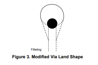
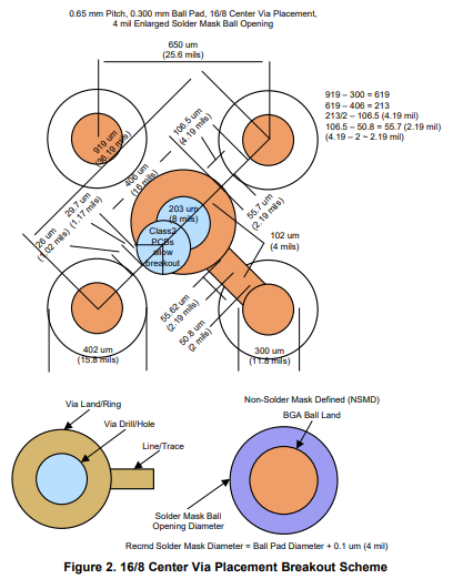 A key advantage of this breakout is reduced PCB costs from 9% to 18% by center locating vias under the SoC and eliminating the non-conductive via fill step. During the via fill step, the via is placed between the balls with a larger land diameter and risks wicking solder into the via from the balls during the soldering process. Another advantage of center locating the via is impedance versus frequency response improves because the power and ground routing is closer to the balls in this scheme. A modified via land shape must be implemented, which is called filleting. The shape looks similar to a tear drop and prevents the via breaking out onto the etch and potentially causing an open at that point.
 2.4.4 Power Distribution Network(PDN)
Refer to Figure 5 of DRA71x Cost Effective Automotive Reference Design User Guide [1] for this reference design.
2.4.4.1 PDN Simulation Results
Refer to Appendix C for simulation results regarding the main SoC power rails. The simulation results for each rail includes effective resistance, loop inductance, ir voltage drop, and target impedance.
2.4.4.2 Power-Up Sequence
Refer to Appendix A for the verified SoC power-up sequence. This sequence has been verified to meet the power-up sequence requirements.
2.4.4.3 Power-Down Sequence
Refer to Appendix B for the verified SoC power down sequence. This sequence has been verified to meet the power-down sequence requirements.
2.4.4.4 Processor PDN
Key device processor high-current power domains must be evaluated for power rail IR drop, decoupling capacitor loop-inductance, and power rail target impedance. A PCB’s PDN performance only be truly accessed by comparing these model PI parameters versus TI’s recommended values. Table 2 shows the recommended values to achieve when conducting a PDN test. These supplies are tests in the included results. For more detailed content, refer to DRA71x Infotainment Applications Processor data sheet [2].
Table 2. Processor Recommended PDN and Decoupling Characteristics
| PDN ANALYSIS | STATUS | DYNAMIC | NUMBER OF RECOMMENDED DECOUPLING
CAPACITORS |
|||||||||
| SUPPLY | MAXIMUM Reff (mΩ) | DECOUPLING
CAPACITORS MAXIMUM LL (nH) |
MAXIMUM
IMPEDANCE (mΩ) |
FREQUENCY
RANGE OF INTEREST ( MHz ) |
100 nF | 220 nF | 470 nF | 1 µF | 2.2 µF | 4.7 µF | 10
µF |
22
µF |
2.4.5 High-Speed Differential (HSD), DDR3L Routing
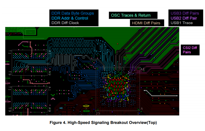
Differential pairs must be etched properly in order to have matching length and coupling. With high-speed interfaces, such as DDR memory, USB3.0, and HDMI, proper etching is crucial especially because a six-layer design has less layers, which leaves less space for all components to be etched on the PCB. When designing the PCB the differential pairs must be laid out first in order to have all the matching lengths and isolation before populating with other etches. Figure 4 shows some of the etching of differential signals on the reference design.
 Article Courtesy: Texas Instruments