


 motor driver solution for a vacuum robot main wheel and main brush)
Description
This reference design demonstrates a brushed DC (BDC) motor driver solution for a vacuum robot main wheel and main brush, which can detect a motor stall without any additional sensors. This design allows for a low component count and small form factor while providing flexibility for controlling BDC motors. The design incorporates enhanced protections like overcurrent, overvoltage, undervoltage, and thermal shutdown.


Features
- Operates at voltages ranging from 4.5 V to 33.6 V
- High output peak current: 3.5 A
- Integrated H-bridge pre-driver and FETs
- Reliable motor stall detection by integrated current sensing
- Overcurrent, short circuit, overvoltage, undervoltage, and thermal protections.
- Operating ambient: –40°C to 85°C
Applications
- Vacuum robot
- Cordless vacuum cleaner
- Refrigerator and freezer
1 System Description
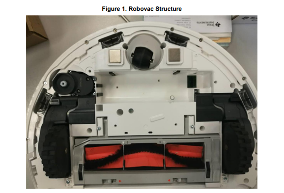
A robotic vacuum cleaner, often called a robovac or roboVac, is an autonomous robotic vacuum cleaner which has intelligent programming and a limited vacuum floor cleaning system. An advantage to using a Robotic Vacuum Cleaner (robovac) is that they vacuum automatically. Brushed DC motors are the popular choice because of the small body size.
The following list shows the general advantages of BDC motors:
- Small size
- Easy to drive
- Cost-effective
2 System Overview
2.1 Block Diagram
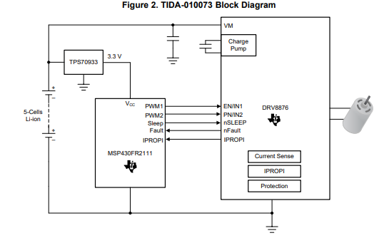
2.2 Design Considerations
This reference design is based on the TI DRV887x family of H-bridge drivers. The control MCU is TI’s MSP430FR2111 which integrates the comparator and a 10-bit ADC.
The DRV887x family of devices are flexible motor drivers for a wide variety of end applications. The devices integrate an N-channel H-bridge, charge pump regulator, current sensing and regulation, current proportional output, and protection circuitry. The charge pump improves efficiency by allowing for both high-side and low-side N-channels MOSFETs and 100% duty cycle support. The family of devices come in pin-to-pin, scalable RDS(on) options to support different loads with minimal design changes. The MSP430FR21xx MCUs feature a powerful 16-bit RISC CPU, 16-bit registers, and a constant generator that contributes to maximum code efficiency.
2.3 Highlighted Products
The following subsections detail the highlighted products used in this reference design, including the key features for their selection. See their respective product data sheets for complete details on any highlighted device.
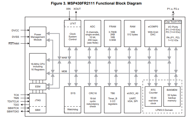
2.3.1 MSP430FR2111
The MSP430FR2111 devices are part of the MSP430 microcontroller (MCU) value line sensing portfolio. This ultra-low-power, low-cost MCU offers memory sizes 4KB of FRAM unified memory with several package options including a small 3-mm × 3-mm VQFN package. The architecture, FRAM, and integrated peripherals, combined with extensive low-power modes, are optimized to achieve extended battery life in battery-powered applications.
The MSP430FR2111 MCU features a powerful 16-bit RISC CPU, 16-bit registers, and a constant generator that contributes to maximum code efficiency. The digitally controlled oscillator (DCO) allows the device to wake up from low-power modes to active mode typically in less than 10 μs.
The MSP430 ultra-low-power (ULP) FRAM microcontroller platform combines uniquely embedded FRAM and a holistic ultra-low-power system architecture, allowing system designers to increase performance while lowering energy consumption. FRAM technology combines the low-energy fast writes, flexibility, and endurance of RAM with the nonvolatile behavior of flash.
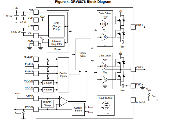
2.3.2 DRV8876
The DRV887x family of devices are flexible motor drivers for a wide variety of end applications. The devices integrate an N-channel H-bridge, charge pump regulator, current sensing and regulation, current proportional output, and protection circuitry. The charge pump improves efficiency by allowing for both high-side and low-side N-channels MOSFETs and 100% duty cycle support. The family of devices come in pin-to-pin, scalable RDS(on) options to support different loads with minimal design changes.
Integrated current sensing allows for the driver to regulate the motor current during start up and high-load events. A current limit can be set with an adjustable external voltage reference. Additionally, the devices provide an output current proportional to the motor load current. This can be used to detect motor stall or a change in load conditions. The integrated current sensing uses an internal current mirror architecture, removing the need for a large power shunt resistor, saving board area and reducing system cost.
A low-power sleep mode is provided to achieve ultra-low quiescent current draw by shutting down most of the internal circuitry. Internal protection features are provided for supply undervoltage lockout (UVLO), charge pump undervoltage (CPUV), output overcurrent (OCP), and device overtemperature (TSD). Fault conditions are indicated on nFAULT.
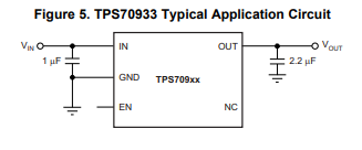
2.3.3 TPS70933
The TPS709 series of linear regulators are ultra-low, quiescent current devices designed for power-sensitive applications. A precision band-gap and error amplifier provides 2% accuracy over temperature. A quiescent current of only 1 μA makes these devices ideal solutions for battery-powered, always-on systems that require very little idle-state power dissipation. These devices have thermal-shutdown, current-limit, and reverse-current protections for added safety.
Shutdown mode is enabled by pulling the EN pin low. The shutdown current in this mode goes down to 150 nA, typical.
The TPS70933 device can be enabled as an optional choice in the reference design to evaluate the ultralow standby power consumption.
2.4 System Design Theory
For the BDC motor driver, usually the control is open-loop. The disadvantage of the simple control is obviously to be seen that the motor will be too hot to be damaged when the motor is blocked to stop. This design can show a solution that detects the motor stall condition without any other additional components. The internal comparator and ADC of MSP430FR2111 will help do the stall detection and motor speed calculation.
- MSP430FR2111 – User interface, speed detection, and software based protection.
- DRV8876 – H-bridge driver, current sensing and hardware protection
- TPS709 – Ultra-low IQ LDO
2.4.1 Motor Speed and Stall Detection
In many BDC electric motor applications, it is essential to keep track of the motor rotations to implement precise and reliable motion control. Traditionally this is done with optical sensors with photodiodes or Hall effect sensors both which pick up counting pulses from the rotating motor shaft or from the movements of the load attached to the motor shaft. These counting pulses are then sent back to the motor controller. To reduce implementation complexity and cost in electric motor applications it is attractive to use sensorless rotation counting methods, that is, methods where sensors and feedback wires with fragile connectors are not required.
2.4.2 Ripple Counting
Ripple Counting is a known sensor-less counting method. This method is based on measuring the fluctuations in the supply current to the motor as it rotates. Ripple Counting works on the ‘law of induction’, or more specifically Lenz’s law, which says that the magnetic field of any induced current opposes the charge that induces it. This so-called Back Electromotive Force (BEMF) (sometimes called the counter electromotive force) can be detected by measuring the current flowing through each coil as the motor rotates. The current measured in-line with the brushed motor has both a large-amplitude, very low-frequency DC component and a small-amplitude, high-frequency AC component.
Both of these components must be considered when choosing the correct configuration for this design. The total current seen in-line with the motor can be solved in Equation 1 as:
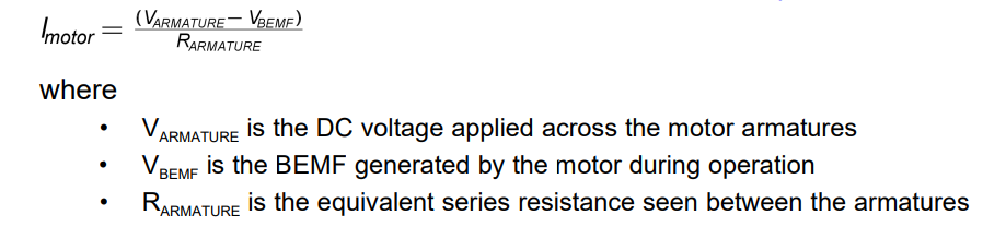
The DC-component current is the main source driving the inductive load of the motor. The motor load varies widely depending on the necessary torque to drive the mechanical motor assembly.
The AC-component current is created by the sinusoidal BEMF generated by the motor, as well as the periodic changes in motor coil impedance due to the motor brushes shorting adjacent commutator poles. The amplitude and frequency of this component also varies both on the mechanical load on the motor and the design of the motor itself. This AC component contains the ripple that the user should measure and is directly proportional to the actual motor speed. Every ripple corresponds to a commutator pole rotation across the armature brushes. The total sub-divisions of a full rotation can be captured by knowing the total number of poles in the motor.
3 Hardware, Software, Testing Requirements, and Test Results
3.1 Required Hardware and Software
3.1.1 Hardware
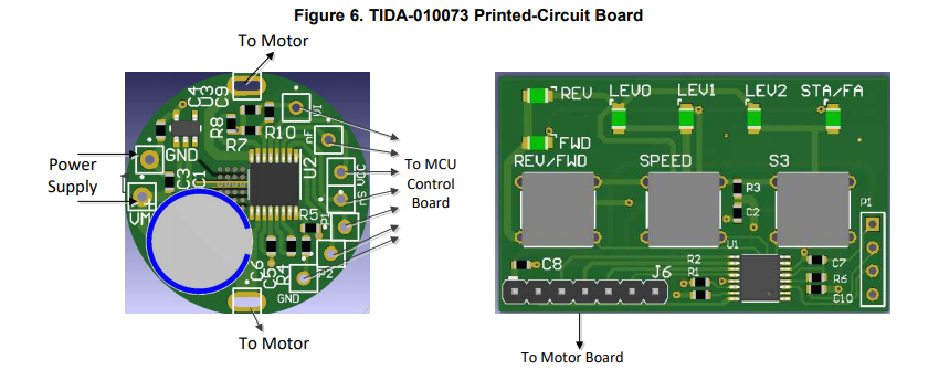
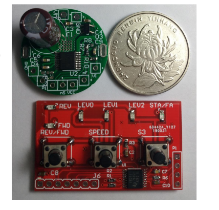
The design includes 2 boards. The 20-mm diameter board is motor driver board which can be directly mounted on the back of the motor. The control board with LED and Key can set the motor speed, rotation detection and show the stall condition.
3.1.2 Software
Programming interface for MSP430 MCU
P1 is reserved as the programming interface for the MCU. The designer can program the MSP430 MCU using the JTAG port, Spy-Bi-Wire (SBW), and the bootloader BSL. In this reference design, SBW has been adopted for programming and is a two-wire SBW interface. Spy-Bi-Wire can be used to interface with MSP430 development tools and device programmers. Table 2 lists the SBW interface pin requirements. For further details on interfacing to development tools and device programmers, see the MSP430 Hardware Tools User’s Guide.
3.2 Testing and Results
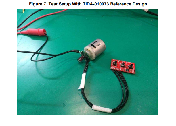
3.2.1 Test Setup
The following steps show how to set up the test platform in the lab during the test:
- Ensure that the firmware has been programmed into the MCU (see Section 3.1.2) in MCU board
- Connect the motor with the 2 motor output pins. Any connection is available.
- Connect the DC power source to the motor board. Keep the power OFF. Set the power output voltage between 16 V and 21 V. Set the current limitation up to 3.5 A. 4. Use the forward and reverse key to start the motor. Use the up and down key to control the motor speed.
3.2.2 Test Results
The test results are listed in the following:
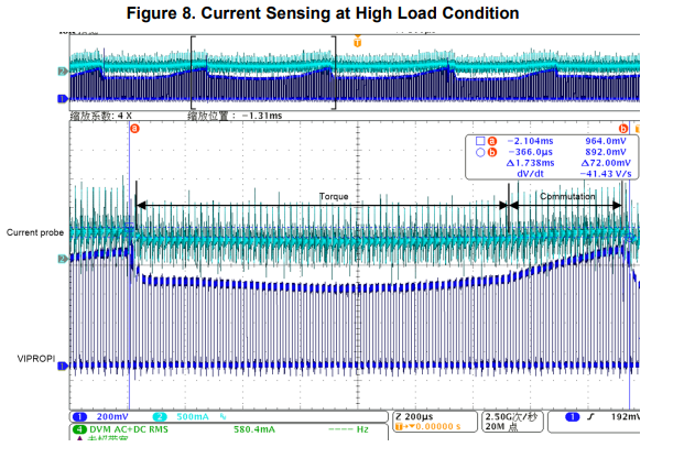
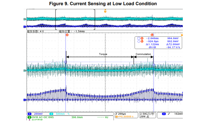
- Current feedback from DRV8876
The DRV8876 integrates output current sensing using current mirrors on the low-side power MOSFETs. A proportional current is then sent out on the IPROPI pin and can be converted to a proportional voltage using an external resistor (RIPROPI). Figure 8 and Figure 9 show the current sense voltage at different loads. Channel 2 is the current probe. Channel 4 is the voltage probe by VIPROPI.
- Speed loop test result
The MCU software samples the phase current at each PWM on stage. The algorithm calculates the normal current based on the current at the torque stage and determines the commutation stage with the current ripple. The software also counts the speed between the 2 commutations.
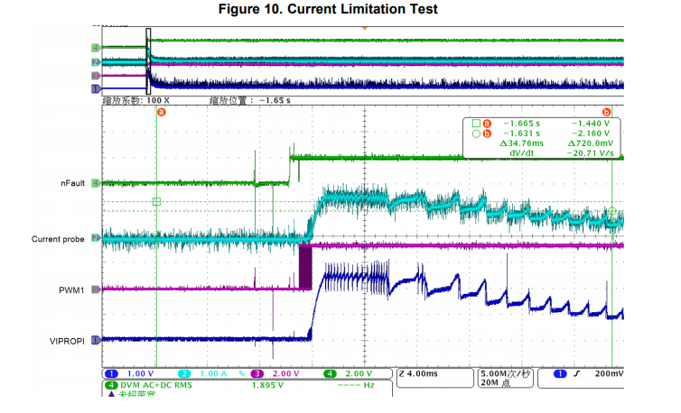
- Current limitation test result
- Protection test result
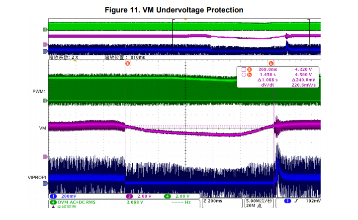
– Undervoltage lockout
The DRV8876 device monitors the VM voltage at any time. If the falling voltage is less than 4.35 V, it stops the output and generates an undervoltage protection. The protection is active until the voltage rises higher than 4.45 V, only then can it return to normal operation. Figure 11 shows the undervoltage protection.
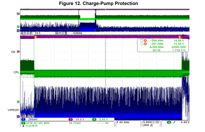
– Charge-pump undervoltage lockout
The DRV8876 device monitors the charge-pump voltage. If the charge pump voltage drops to 2.25 V, the hardware stops the output and generates a fault signal. After the charge-pump voltage is returned, the output can be recovered. Figure 12 shows the charge-pump protection.
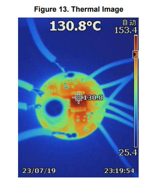
- Thermal test
To better understand the temperature of power components and the maximum possible operating temperature, the thermal images were plotted at room temperature (25°C) with a closed enclosure and at 100% duty output conditions.
About the Author
Fan (Hawken) Li is a systems engineer at Texas Instruments, where he is responsible for developing reference design solutions for the industrial segment. Hawken brings to this role his extensive experience in home appliances, including motor driver, EP, analog circuit design, and so forth.
For more information, visit: www.ti.com