


Designers of power systems face constant pressure from the market to make the most efficient use of the available power.
In portable devices, greater efficiency extends battery life and allows more features to be packed into smaller packages. In servers and base stations, greater efficiency leads directly to savings both in infrastructure (the cooling system) and operating costs (the power bill).


In response, system designers are improving the power conversion process in several areas, including more efficient switched-mode topologies, packaging innovations, and new semiconductor devices based on silicon carbide (SiC) and gallium nitride (GaN).
Improvements in Switching Converter Topologies
The push to make the most of the available power has led to the increasing adoption of designs based on switching, rather than linear, technology. Switched-mode power supplies (SMPSs) can attain efficiencies greater than 90%. That extends battery life in portable systems, reduces electricity costs in large installations, and frees up space formerly devoted to heat dissipation components.
The move to switching topologies has a downside, though, in the form of a more complicated design that demands a diverse set of skills. The design engineer must be familiar with analog and digital techniques, magnetics and closed-loop control. The printed circuit board (PCB) designer must pay more attention to electromagnetic interference (EMI) because the high-frequency switching waveforms can cause problems in sensitive analog and RF circuits.
The basic concepts behind switched-mode power conversion predate the invention of the transistor: the Kettering inductive discharge system, for example, was invented in 1910 and used a mechanical vibrator to implement a flyback boost converter for automotive ignition.
Most of the standard topologies have been around for decades, but that does not mean that engineers aren’t tweaking the standard designs, particularly in the control loop, to accommodate new applications. The standard architectures use fixed frequencies and maintain a constant output voltage under varying load conditions either by feeding back a portion of the output voltage (voltage mode control) or by controlling the inductor current (current mode control). Designers have developed refinements to overcome the shortcomings of the basic designs.
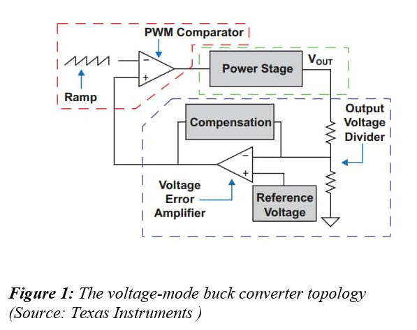
Figure 1 shows a block diagram of the basic closed-loop voltage mode control (VMC) system. The power stage consists of the power switches and output filter. The compensation block includes the output voltage divider, an error amplifier, voltage reference and loop compensation components. The pulse width modulator (PWM) uses a comparator to compare the error signal to a fixed ramp, creating an output pulse train that has a width proportional to the error signal.
Although the VMC system provides tight output regulation with varying loads and is easy to synchronize to an external clock, the standard architecture has several drawbacks. The loop compensation decreases the control loop bandwidth and slows transient response; the error amplifier increases operating current and reduces efficiency.
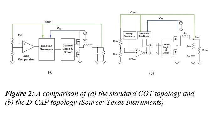
The constant-on-time (COT) control scheme provides good transient performance without the need for loop compensation. This COT control uses a comparator to compare the scaled output voltage with a reference voltage: whenever the output is less than the reference, a fixed on-time pulse is generated. This can result in a very high switching frequency during low duty ratio conditions, so the adaptive COT controller generates an on-time that varies as a function of input and output voltage; this maintains a nearly constant frequency during steady-state conditions.
Texas Instruments’ D-CAP topology is a refinement of the adaptive COT method: the D-CAP controller adds a ramp voltage to the input of the feedback comparator. The ramp improves the jitter performance by reducing the noise band in the application. Figure 2 compares the COT and D-CAP systems.
 There are several variants of D-CAP topology optimized for different requirements. The TPS53632 half-bridge PWM controller, for example, uses the D-CAP+ architecture, designed for high-current applications, to drive a power stage at up to 1MHz to give an efficiency as high as 92% in a 48V to 1V POL converter.
In contrast to D-CAP, the D-CAP+ feedback loop adds a component proportional to the inductor current for accurate droop control. An added error amplifier improves DC load accuracy under varying line and load conditions.
The controller’s output voltage is set via an internal DAC. The cycle begins when the current feedback reaches an error voltage level corresponding to the amplified difference between the DAC set point voltage and the feedback output voltage.
Improved Operation Under Light Load Conditions
The move to portable and wearable equipment has led to a need for improved performance under light load conditions to extend battery run time. Many portable and wearable applications spend most of their time in a low-power standby “snooze” or “sleep” mode, waking up only to respond to a user input or take a periodic measurement, so minimizing power consumption during standby mode is a top priority.
The DCS-Control (Direct Control with Seamless Transition into Power Save Mode) topology combines the advantages of three different control schemes—hysteretic, voltage mode and current mode—to provide improved performance under light load conditions, especially during the transition into and out of the light load state. The topology supports PWM mode for medium and heavy loads, and a Power Save Mode (PSM) for light loads.
During PWM operation, the system operates at its nominal switching frequency with a controlled frequency variation depending on the input voltage. If the load current decreases, the converter switches to PSM to maintain high efficiency down to very light loads. In PSM the switching frequency decreases linearly with the load current. Both modes are the function of a single control block, so the transition from PWM to PSM is seamless and does not affect the output voltage.
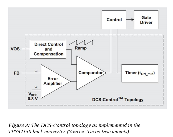
Figure 3 shows the DCS-Control block diagram. The control loop takes information about output voltage changes and feeds it directly to a fast comparator stage. The comparator sets the switching frequency, which is constant for steady-state operating conditions and provides immediate response to dynamic load changes. A voltage feedback loop provides accurate DC load regulation. The internally compensated regulation network achieves fast and stable operation with small external components and low ESR capacitors.
 New Packaging Techniques Help Designers Boost Power Density
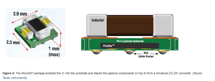
Another way to increase power density is to reduce the size of the PCB area needed. One way to do that is by combining components in a DC/DC module. The MicroSiP and MicroSiL power modules from Texas Instruments integrate the passive components and the integrated circuit (IC) for the power converter into a single device by embedding the IC into an FR4 laminate substrate and mounting the inductor on top of the substrate material.
The fully integrated MicroSiP power modules integrate both IC and passive components into a single device that gives the highest integration level. The smallest modules use the BGA format and can achieve a footprint of less than 7mm².
 A MicroSiL device integrates the power inductor and the regulator IC and uses external capacitors. The module pinout and outline are similar to a QFN-type package. The TPS82085 power module, for example, is a synchronous step-down converter that can deliver 3 A from an eight-pin package measuring 3mm × 2.8mm.
Integration can drastically reduce the footprint, but there are always trade-offs to be considered. For example, the MicroSiP package stacks the inductor on top of the controller and mounts the components on a PCB. Each of these features increases the height of a MicroSiP module compared to a discrete design.
Designing for minimum footprint also requires reducing the size of the inductor. The inductance of a coil is proportional to both its area and the number of turns, so reducing the area without changing inductance forces an increase of wire used. More wire increases the coil’s DC resistance.
Moving Beyond Silicon: SiC and GaN Devices
The quest for higher performance is leading designers to look beyond silicon to other materials. Power devices made from SiC and GaN are starting to replace silicon devices in some power applications; both are examples of wide bandgap (WBG) semiconductors.
In case it has been a while since your last solid-state physics class, the bandgap of a solid is a measure of the energy difference in electron volts (eV) between the top of the valence band and the bottom of the conduction band, and is a major factor determining a material’s electrical conductivity.
In contrast to silicon, which has a bandgap of 1.1eV, WBG semiconductors have bandgaps of 3.3V (SiC) and 3.4V (GaN), so more energy is required to move an electron from the valence band to the conduction band. This has advantages for power semiconductors: compared to silicon, WBG devices have lower on- resistance, higher breakdown voltage, superior reverse recovery characteristics, and can operate at higher switching frequencies.
Higher switching frequencies allow the use of smaller capacitors, inductors and transformers, with size, weight and cost savings. There are electrical benefits, too, with up to 10% improvement in DC-DC conversion efficiency.
Combining WBG semiconductors with advanced packaging, Texas Instruments recently announced the LMG5200, a half-bridge power stage that integrates two 80V GaN power FETs and a high-frequency GaN driver into a single QFN package. The LMG5200 will pair up with existing products, such as the TPS53632, to serve a variety of applications, including synchronous buck converters and 48V POL converters for computing, industrial and telecom applications.
Conclusion
Increasing the efficiency and power density of power conversion solutions requires a multi-disciplinary approach that draws upon expertise in controller design, packaging and semiconductor research. Only by combining advances in all areas can designers meet demand across the broad spectrum of applications, from low-power battery-drive wearables and portables to high-power telecom switches and data centers.
Article Courtesy: Mouser Electronics