Moore’s Law scaling is slowing down and limited improvements in performance, power, area, and cost are available from one process node to the next. As a result, advanced packaging and 3D stacking technologies are taking a front seat as the key drivers for next-generation high-performance energy-efficient designs. These types of system-in-package (SiP) technologies require designers to reimagine system-on-chips (SoCs) and “disaggregate” large monolithic systems into separate chips (or chiplets) on the same or different technology. These chiplets are purpose-built to be assembled in a 2.5D or 3D configuration with an underlying common interconnect medium. Designing a system in this way can result in significant cost savings compared to a monolithic die. 3D stacking, itself, has an extra advantage over 2.5D. It can enable significantly higher bandwidth and lower latency between stacked dies because of its vertical connections. This has been an area of active research by academia and industry over the past few decades. Questions have been raised regarding the feasibility, yield and cost of high-density 3D technologies, 3D-IC design enablement infrastructure, 3D-test, and more. After a few years of conducting simulation-based explorations into 3D-ICs, Arm Research decided that these questions could best be answered by building a demonstrator. This required a strong collaboration between design, electronic design automation (EDA), and manufacturing.
To make that demonstrator a reality, Arm partnered with GLOBALFOUNDRIES to tape-out a 3D prototype design in 2019. Named Project Trishul, the goal was to demonstrate the feasibility and readiness of high-density, face-to-face, wafer-bonded 3D stacking technologies for high performance, energy-efficient designs. Figure 1 shows the piece of a representative Arm Neoverse system the team investigated, and a block diagram of the subsystem components that were demonstrated in 3D. We are happy to announce that the 3D hybrid-bonded chips are back from fabrication, and we have run comprehensive tests to measure and characterize them. The key learnings and measurement results were published at the International Electron Devices Meeting 2020 (IEDM), the premier conference for reporting technological breakthroughs in areas of semiconductor and electronic device technology, design, manufacturing, physics, and modeling.


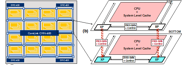
Figure 1: Arm Neoverse CMN-600 and a 2×2 mesh implemented in 3D. Only the “XP” blocks (NoC mesh router) blocks in blue and white are implemented in the test-vehicle.
Through the 3D test-vehicle (whose GDS and die shots are shown in Figure 2), we validated our solutions across a multitude of challenges associated with 3D stacking. Namely:
- Readiness of high-density 3D stacking technologies:We showcased a synchronous cache-coherent mesh interconnect operational at frequencies up to 2.4GHz and partitioned in 3D using 5.76µm-pitch hybrid wafer-bond 3D connections on a 12nm FinFET process.
- 3D EDA:This is the first 3D test-vehicle designed using a novel 3D implementation flow that allows co-optimization of logic gates and 3D connections across the two tiers. The flow is compatible with industry standard EDA tool flows.
- 3D test:The test-vehicle serves as the first known implementation of the IEEE 1838 3DIC Design-for-Test (DFT) standard.
- Bandwidth and energy:We demonstrated a 3D aggregate bandwidth of 307 GB/s, a record bandwidth density of 3.4 TB/s/mm2, and an energy efficiency of 0.02 pJ/bit for the 3D stacked dies.
- Bump-less and PHY-less design: 3D wafer-bond RC parasitics are comparable to that of on-chip global wires. This means signaling across the 3D interface does not require special interface circuits, and can be driven using CMOS logic gates. Additionally, we measured gate delay across the 3D dies to be of the order of 2D logic-gate delays (<20 picoseconds!).
- 3D bond yield and reliability:We showcased measurement and analysis data from 945 bonded die-pairs. A total of 13.5 million signal 3D-wafer-bond nets and 20 million power-delivery 3D-wafer-bond nets from multiple wafer-bonded pairs were tested.
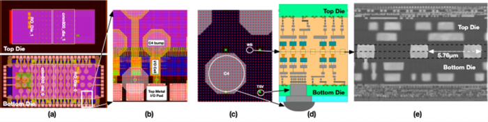
Figure 2: (a) Top and bottom die GDS view (b) zoom-in view showing I/O cell connected to top-metal peripheral pads for pre-bond testing and back-side C4 bumps using Through-Silicon-Via (TSV) for post-bond 3D tests (c) C4 bumps, TSV and wafer-bond pads top-view (d) cross-sectional schematic view and (e) corresponding die cross-section from the 3D test-vehicle
The key learning that we validated from this 3D test-vehicle was that, from an electrical-connectivity perspective, face-to-face hybrid bonding technology does not introduce any significant delay penalty. If the cross-die process skew can be managed, a single clock domain synchronous design with an order of magnitude higher bandwidth and lower energy, compared to state-of-the-art bump-based die stacking techniques, can be implemented. 3D stacking can significantly improve on-chip memory capacity and bandwidth, and can also improve the overall throughput of the system, all while potentially reducing costs.
Based on our findings, we are actively exploring opportunities for 3D-focused architectures that improve SoC performance, power, and cost, while simultaneously addressing the challenges around power delivery and thermal management. We believe high-density 3D stacking technologies complemented with heterogeneous integration will usher in an era of next generation high-performance and energy-efficient systems beyond the current Moore’s Law 2D scaling paradigm.